IBM's Quantum Fab Anderon Targets TSMC-Style Role for Qubits
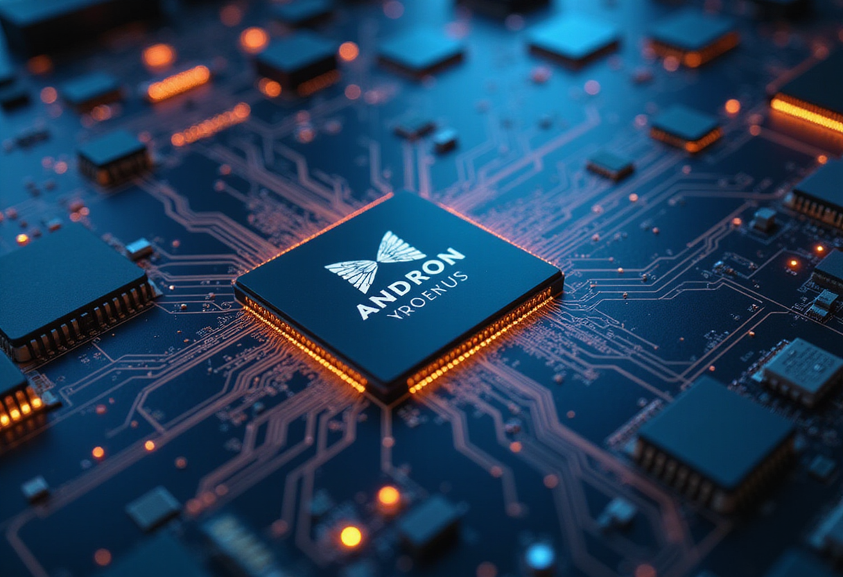
IBM has branded a new quantum-chip fabrication facility 'Quantum Fab Anderon' with the explicit goal of becoming 'the TSMC of qubits,' according to IEEE Spectrum, signaling a foundry-style push for superconducting processors.
- By
- Grace Kim
- Filed
- Channel
- Chip Manufacturing
- Read
- 3 min read
IBM has named a new quantum-chip fabrication facility "Quantum Fab Anderon" with the stated goal of becoming "the TSMC of qubits," IEEE Spectrum reported. The framing marks a deliberate move by IBM to package superconducting quantum-processor manufacturing as a service that outside designers could buy, mirroring the foundry role Taiwan Semiconductor Manufacturing Co. plays in classical semiconductors.
What does "TSMC of qubits" mean?
TSMC's commercial model rests on a single discipline: building chips designed by others, at scale, on processes TSMC itself defines. If IBM replicates that structure for quantum hardware, the company would sell its fabrication know-how, cleanroom capacity, and packaging expertise to outside quantum teams that today build their own processors in-house.
The analogy is precise. TSMC did not invent the smartphone SoC, the discrete GPU, or the network switch ASIC, yet it manufactures the silicon that powers each category. A quantum equivalent would mean IBM would not necessarily own the end-user application stack, the algorithm library, or the cloud interface, but it would own the line that turns qubit designs into physical chips.
Why a foundry model for quantum now?
Quantum hardware teams today duplicate one another's fabrication work. Each lab, startup, and hyperscaler operates its own small cleanroom, refining its own Josephson-junction process and its own cryogenic test recipe. A shared facility would consolidate that learning the way TSMC consolidated CMOS process development over four decades.
The economic logic follows classical-chip history. Yield learning, mask-set reuse, and shared tool depreciation reward scale. A quantum fab serving dozens of customer designs can spread cryogenic-test costs and lithography-tool amortization across a wider base than any single team's captive line.
What it would take to pull off
Naming a facility is the easy step. A genuine quantum foundry would need published process design kits, reproducible yield metrics, and multi-project wafer runs, the way TSMC runs its university shuttle service for academic and small-customer designs at mature nodes. Quantum adds one more layer classical fabs do not face: every chip must be tested at millikelvin temperatures before it ships, which means the fab must integrate dilution-refrigeration test capacity, not just cleanroom capacity.
A second challenge is standards. Today's qubit layouts, control electronics, and cryogenic packaging are not portable between vendors. A foundry can succeed only if it defines a stable interface that customers can target, much as the standard-cell library and PDK format let a fabless chip company move from one TSMC node to the next.
How the competitive picture shifts
If Quantum Fab Anderon opens to outside customers ahead of rivals, IBM could define the de facto boundary between quantum designers and quantum manufacturers. If the line stays internal, the foundry label is branding rather than business. IEEE Spectrum's report does not specify which path IBM has chosen, when third-party runs would start, what wafer capacity the fab carries, or whether any external customer has signed on.
What changes for the supply chain
A merchant quantum foundry would create a new tier in the chip industry, sitting between today's captive fabs and the merchant foundries that handle leading-edge silicon. Component suppliers, from cryogenic interconnects to dilution-refrigeration feedthroughs, would gain a single large customer with predictable process flows. Software stacks would have to standardize as well, since porting a qubit layout between foundries is harder than porting a Verilog netlist between process nodes.
What to watch next
The next milestones will be commercial rather than technical. Watch for published PDKs, announced outside-customer tape-outs, and pricing for multi-project wafer runs at Quantum Fab Anderon. The shift from internal research line to merchant foundry, not the qubit count of any single chip IBM ships, will determine whether the TSMC comparison holds.
Source: Google News: semiconductors
More from Grace Kim
Show full bio
Market editor covering industry trends and analytics at Chip Dispatch.
278 articles
Related articles
tsmc-shares-climb-on-report-of-broadcom-s-60-billion-chip-commitment-9326ac56
TSMC Shares Climb on Report of Broadcom's $60 Billion Chip Commitment
globalfoundries-to-build-silicon-interposers-for-tsmc-6d577db4
GlobalFoundries to Build Silicon Interposers for TSMC
globalfoundries-to-manufacture-key-ai-chip-component-for-tsmc-46e9e28e
GlobalFoundries to Manufacture Key AI Chip Component for TSMC
tsmc-turns-to-taiwan-partners-one-fab-giant-can-t-meet-ai-demand-alone-538ebd95
TSMC Turns to Taiwan Partners: One Fab Giant Can't Meet AI Demand Alone
![[Taiwan Chip News] "Can't Keep Up Alone"... Why TSMC Is Rallying Domestic Partners - 아시아경제](/media/2026/09/b634f534cfd658a7.png)