Intel and TSMC Share R&D Floor at Applied Materials EPIC Center
Intel and TSMC, direct foundry competitors at the 3nm and 2nm logic nodes, now share wafer R&D space inside Applied Materials' EPIC Center in Santa Clara, California, per trade-press coverage.
- By
- Sophie Lindqvist
- Filed
- Channel
- Chip Manufacturing
- Read
- 3 min read
Intel and TSMC — direct foundry competitors at the 3nm and 2nm logic nodes — now run wafer R&D on a shared floor inside Applied Materials' EPIC Center in Santa Clara, California, according to a Tech Times report circulating through trade channels this week.
The arrangement places the two chipmakers on a single equipment-evaluation line inside Applied Materials' flagship research campus. Neither company has publicly confirmed the arrangement.
Applied Materials declined to disclose which process nodes, tool families, or wafer sizes are under evaluation. No deal value, rental figure, or exclusivity term has appeared in any SEC filing.
Why are Intel and TSMC working under one roof?
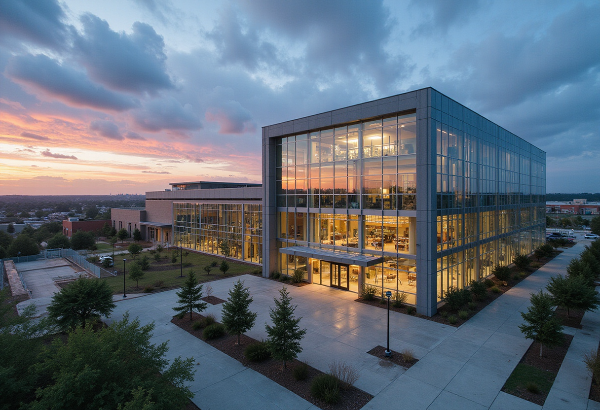
The EPIC Center — formally the Equipment and Process Innovation and Commercialization Center — houses one of the industry's largest non-production research cleanrooms. Chipmakers use the facility to qualify deposition, etch, inspection, lithography, and packaging tools before committing them to commercial fabs.
Applied Materials opened the roughly 110,000-square-foot facility in 2017 as part of a multi-hundred-million-dollar build-out. Co-locating rival customers on a vendor's neutral site is a long-standing industry practice.
Chipmakers save the cost of building duplicate evaluation lines. Equipment suppliers shorten tool-tuning cycles. EPIC has hosted R&D sessions from major logic and memory chipmakers since opening.
Both Intel and TSMC rank among Applied Materials' largest equipment customers by revenue. Industry analysts place Applied Materials at the top of the deposition and chemical-mechanical planarization segments. Tokyo Electron and Lam Research hold dominant positions in adjacent process steps.
What changes for production roadmaps?
The shared EPIC presence leaves neither company's public production roadmap visibly altered. TSMC's Arizona Fab 21 — its first U.S. leading-edge logic fab, producing 4nm wafers — remains on its disclosed ramp schedule.
Intel's 18A node, the company's first sub-2nm-class logic process, is in volume-production preparation at fabs in Oregon and Arizona. The equipment spending behind those nodes is substantial.
TSMC's 2025 capital expenditure guidance sits near $40 billion, with U.S. expansion consuming a meaningful share. Intel's 2025 capex guidance runs roughly $20 billion, with significant dollars allocated to process development and equipment qualification. Applied Materials does not break out per-customer revenue.
What about CHIPS Act and antitrust review?
Regulators are positioned to take notice. The U.S. Department of Commerce administers CHIPS and Science Act provisions governing joint research among award recipients. Intel, TSMC, and Applied Materials are all listed CHIPS Act awardees. The department has authority to review whether shared R&D access qualifies as in-scope collaboration.
Competition lawyers may also weigh in. Direct collaboration on equipment process recipes between two active foundry competitors can raise antitrust scrutiny. Vendor-mediated co-location has historically been treated as a routine commercial arrangement.
Both chipmakers now operate active foundry service platforms — Intel Foundry and TSMC — competing for external customer wafers at nodes including 3nm, 4nm, and 2nm. The co-presence at EPIC blurs that rivalry only at the equipment-research layer.
For now, both companies gain faster feedback on Applied Materials' tool roadmap, and the vendor gains an additional demand signal as U.S. foundry capacity expansion accelerates under federal incentives.
As competition tightens through 2026 and domestic 4nm, 3nm, and 2nm-class wafer output scales up, the EPIC co-presence will shape how quickly each side qualifies the tools underpinning its next fabs.
Source: Google News: TSMC
More from Sophie Lindqvist
Related articles
tsmc-prepares-to-pour-265-billion-into-u-s-fab-buildout-762fb55c
TSMC Prepares to Pour $265 Billion Into U.S. Fab Buildout
tsmc-weighs-multibillion-dollar-texas-campus-for-ai-chip-output-7e33d191
TSMC Weighs Multibillion-Dollar Texas Campus for AI Chip Output
tsmc-s-265-billion-arizona-bet-reshapes-enterprise-chip-sourcing-bdccc3b6
TSMC's $265 Billion Arizona Bet Reshapes Enterprise Chip Sourcing
tsmc-weighs-multibillion-dollar-texas-campus-to-expand-ai-chip-capacity-3e064d8a
TSMC Weighs Multibillion-Dollar Texas Campus to Expand AI Chip Capacity