Micron’s G11 3D NAND targets 42 Gb/mm² and 5,400 MT/s in 2027
Micron plans a 2H 2027 ramp for G11, promising more than 400 layers, 42 Gb/mm² bit density, 5,400 MT/s I/O and over 25% lower data-transfer energy per bit.
- By
- Nathan Brooks
- Filed
- Channel
- Memory & Storage
- Read
- 4 min read
By Nathan Brooks
Micron plans to begin mass production of its G11 3D NAND in the second half of 2027, targeting more than 400 layers, 42 Gb/mm² bit density and a 5,400 MT/s interface. The company expects the device to approximately double the bit density of G9 and raise I/O performance by 50%. All three specifications remain targets, not results from shipping devices.
At an event this week, Micron presented G11 as a major successor to its current G9, also called N160, generation. G11 uses 3D TLC and targets 42 Gb/mm², compared with 21 Gb/mm² for G9. These are company projections rather than independently measured results from G11 devices.
That distinction matters for commercial claims. Micron described the density gain as dramatic relative to Kioxia’s BiCS10 and Samsung’s V10, but provided no comparable density figures for those products. A roadmap target is not yet a benchmark win. Micron plans to disclose more technical details in 2027, close to high-volume manufacturing.
What does G11 promise?
Micron set out three principal goals for G11:
- Density: approximately twice G9’s bit density, reaching 42 Gb/mm² for 3D TLC.
- I/O: up to 50% higher interface speed, rising from 3,600 MT/s to 5,400 MT/s.
- Energy: more than 25% less data-transfer energy per bit.
The targets cover conventional high-capacity SSDs for client and data-center applications. Micron also sees G11 serving emerging AI-oriented storage devices that require greater bandwidth and energy efficiency.
How does wafer bonding fit?
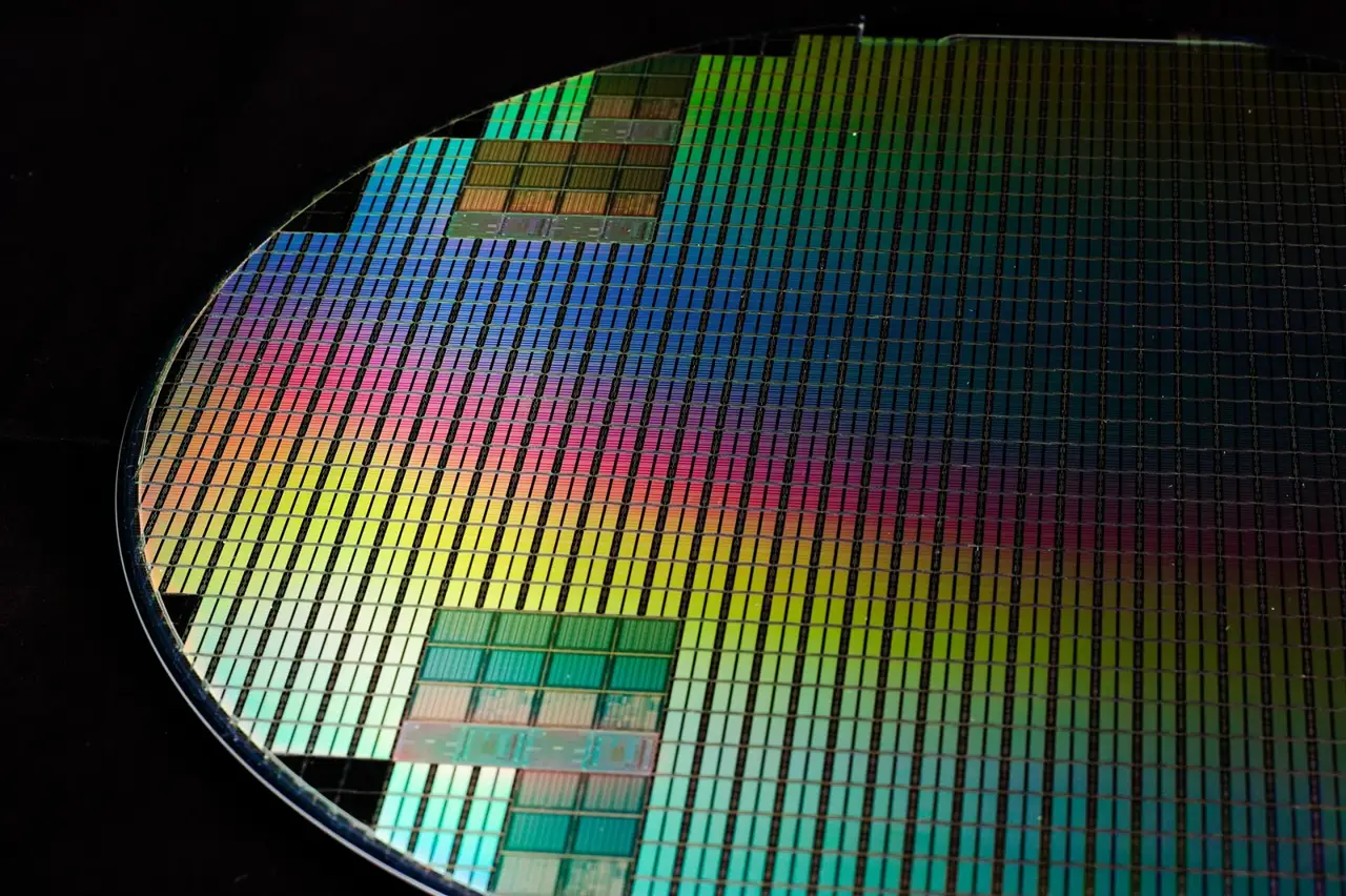
Micron will fabricate the NAND array on a new 3D NAND process, while making peripheral circuits and I/O with a separate logic fabrication process. It will then bond the wafers together. The approach follows YMTC’s use of the technique, extending beyond the CMOS-under-array architectures Micron has used for several generations.
Wafer bonding lets Micron optimize the memory array and peripheral logic independently. If the plan works as intended, that separation should support more capacity and performance.
Scott DeBoer, Micron’s president and chief technology and products officer, said the company had waited to introduce wafer bonding until it was cost-effective and useful for product specifications. He added: “This G11 technology is the world’s most advanced NAND.” The ranking is Micron’s claim, not an independently measured result.
More than 400 NAND layers will provide part of the density gain, while Micron’s claimed industry-leading memory cell pitch points to smaller cell dimensions as well. The company has not disclosed G11’s exact number of active wordline layers or memory decks. It expects to publish more technical detail in 2027, close to high-volume manufacturing.
Can client SSDs become cheaper?
The disclosed specifications make a more capacious client SSD plausible, especially if G11 reaches its density and power targets during volume production. They do not establish a retail price reduction. Micron has offered no SSD capacities, product pricing or customer deployment schedule, so claims of an immediate cost advantage would run ahead of the announcement.
For data-center and AI storage, the more immediate promise is throughput and lower transfer energy, not merely more layers. That matches the bandwidth and efficiency requirements Micron expects from emerging AI-oriented devices. Kioxia’s BiCS10 and Samsung’s V10 remain the competitive references in the company’s own framing.
What comes after G11?
Micron says its next steps include high-mobility materials, ultra-dense cell architectures and more energy-efficient devices and data paths. The company believes these developments could improve transistor characteristics, shrink memory cells further and reduce the energy used to move data inside NAND.
DeBoer said: “Beyond G11, we have a strong roadmap ... focused on new materials densifying the cell architecture, and continuing to focus on that XYZ scaling going forward.” The industry direction, he added, combines added layers with smaller cell dimensions.
Conventional 3D NAND scaling began mainly by stacking layers. Future generations also need X- and Y-axis cell reductions to improve density while keeping manufacturing complexity in check.
Micron has disclosed no density targets, detailed architectures or production schedules for post-G11 products. Its roadmap points instead to a broader engineering contest among materials, cell design and peripheral circuitry.
The layer-count race is also likely to continue because active layers remain an easy density lever and demand for 3D NAND-based storage remains strong. Layer count, however, will be an incomplete measure of technology leadership.
If Micron delivers G11 on schedule in 2027, its 42 Gb/mm² density and 5,400 MT/s interface will give client and data-center SSDs more capacity and faster transfers. For buyers, more capacity looks firmer than lower prices; wafer bonding must prove that added capability also lowers cost at volume.
Source: Tom's Hardware
More from Nathan Brooks
Show full bio
Senior reporter covering people, launches and day-to-day practice in Semiconductors, chip manufacturing, hardware, AI compute at Chip Dispatch.
740 articles
Related articles
samsung-unveils-gen-10-v-nand-and-256tb-qlc-flagship-at-gmif2026
Samsung Unveils Gen 10 V-NAND and 256TB QLC Flagship at GMIF2026
sandisk-nas-800-review-14pbw-endurance-at-a-45-65-price-premium-a661de8b
Sandisk NAS 800 Review: 14PBW Endurance at a 45-65% Price Premium
micron-aims-eim-memory-chip-mass-production-115a8dca
Micron Aims EIM Memory Chip at 2028 Mass Production
micron-pledges-250-billion-for-us-fab-buildout-through-4b88b416
Micron Pledges $250 Billion for US Fab Buildout Through 2035