Microsoft's Maia 300 Pushes 12,288 XPUs Into One Coherency Domain
Microsoft's Maia 300 'Clea' XPU packs 288 GB of HBM4, 12,288-XPUs coherency domains, and 7X token throughput at 2.5X better efficiency — detailed at OCP Summit 2026.
- By
- Rebecca Stone
- Filed
- Channel
- AI & Compute
- Read
- 4 min read
By Rebecca Stone, Chip Dispatch
Microsoft's third-generation Maia 300 inference XPU — code-named "Clea" — delivers up to 7X the token throughput of a Maia 200 rack while improving performance per watt by 2.5X, according to Rani Borkar, president of Azure Hardware Systems and Infrastructure, and Saurabh Dighe, corporate vice president of Systems Planning and Architecture, who detailed the chip at the Open Compute Project Summit 2026 this week.
That 7X figure is the number Microsoft is likely most proud of. It's easy to get more performance by throwing more power at a problem. It's another thing entirely to do it while raising efficiency.
What's actually inside the package?
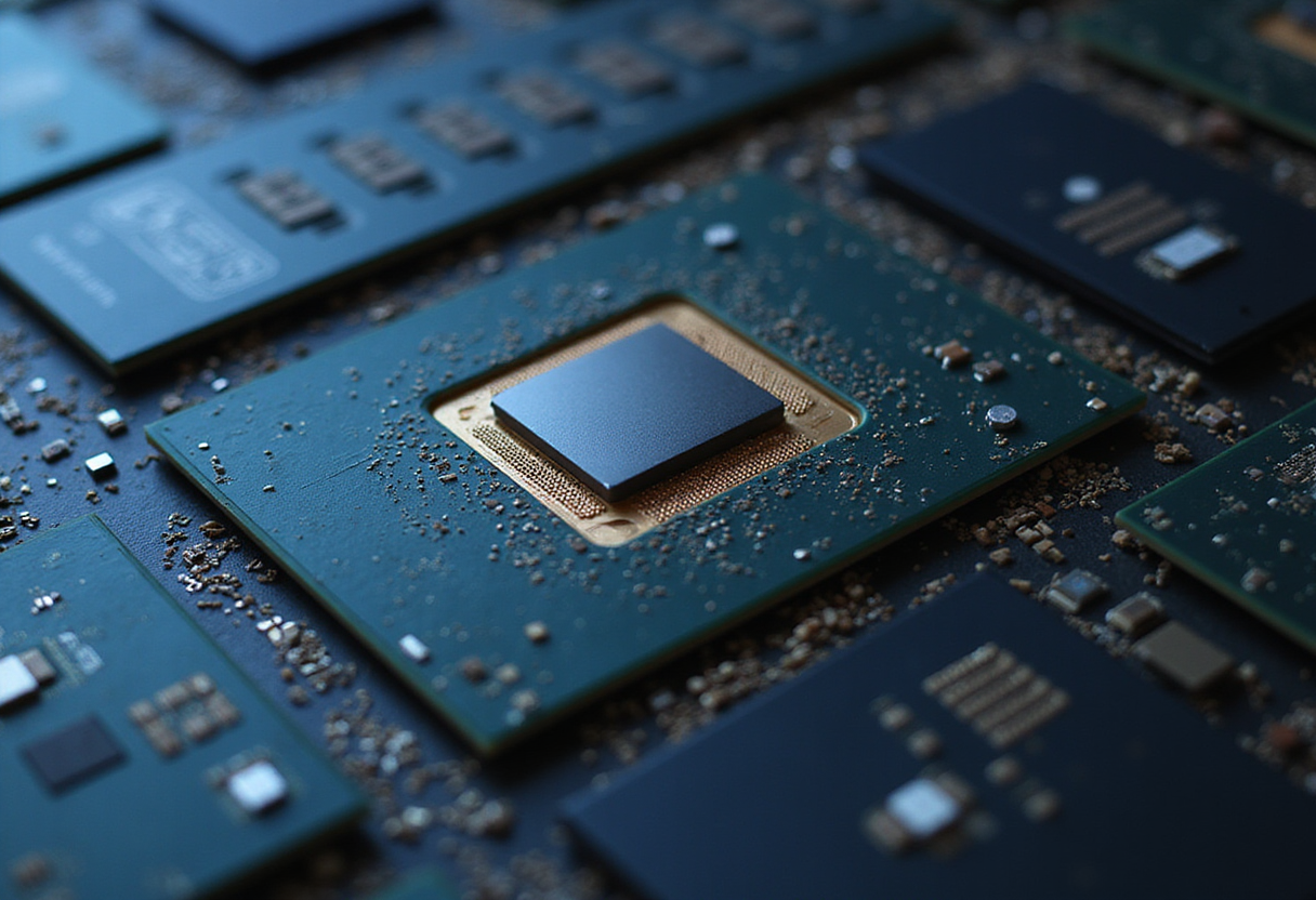
The Clea device isn't a monolithic system on chip. It's a collection of seven dies and eight HBM4 stacks on an interposer — a system in a socket, effectively. Microsoft moves from TSMC's 3nm N3P node, used for the Maia 200 "Braga," to the 2nm N2P process, and for the first time breaks out I/O and HBM controllers into separate chiplets from the compute and SRAM cache elements.
The architecture keeps four tile clusters, just like Maia 200, but each cluster now carries twelve tiles instead of ten. Microsoft hasn't disclosed SRAM capacities, but a reasonable estimate puts roughly 400 MB of SRAM across the central compute die and around 200 MB more in the I/O chiplets — guesses, clearly labeled as such.
The confirmed bandwidth figure is 18 TB/sec of HBM bandwidth feeding 288 GB of HBM4, presumably from SK Hynix as it was with Braga. Aggregate SRAM bandwidth likely lands near 166.2 TB/sec. The package measures roughly 1,980 mm² — about 2.4X the estimated 810 mm² of Braga — with a transistor count plausibly around 280 billion, plus or minus 10 percent, excluding the HBM4 stacks.
Microsoft hasn't named its chip shepherd for Maia 300. Global UniChip of Taiwan, 35 percent owned by TSMC, shepherded Maia 100, and everyone presumes GUC carries the follow-ons — though rumors have circulated about both Marvell and Broadcom angling for the Microsoft custom silicon business.
Where did Maia come from?
Microsoft dipped its toe in the water with the "Athena" Maia 100 in November 2023, alongside the Cobalt 100 Arm server CPU, saying little about either. The second-generation Braga, unveiled this January, is the chip ramping on Azure now.
Scott Guthrie, executive vice president of Cloud and AI at Microsoft, said the "multigenerational Azure Maia program has become a foundational element of Microsoft's AI infrastructure strategy," and that Maia 200 is doing inference for Copilot, with GitHub Copilot and Microsoft Foundry shifting to Maia 200s by year's end. Maia 200s will run OpenAI's models, Microsoft's own, and open source models through Foundry.
Guthrie also said Maia will see "multi-gigawatt deployments" on Azure. The rumor mill puts the ambition at least 1 million Maia sockets in the field. One gigawatt of Maia 300s works out to about 575,000 devices, all in at 1.74 kW per accelerator plus its share of host, storage, and networking.
How big is the coherency domain?
Big. A rack of Maia 300s carries 96 XPUs across 24 1U servers — double the 48 XPU racks of Braga, thanks to the shift from 2U — and burns about 167 kW with liquid cooling. Lash 128 racks together with the new ATL 2.0 Ethernet network and you get 12,288 accelerators in a single system image.
That's the largest coherency domain yet disclosed among the big cloud builders, dwarfing the 72- and 144-GPU domains Nvidia and AMD ship today, and even the 576 or 1,152 multi-tiered NVSwitch fabrics Nvidia has promised. Google's unshipped "Sunfish" TPU 8t tops out at 9,600 TPUs per domain.
Microsoft also changed the memory topology. Braga shared all HBM across all compute tiles and tightly coupled four XPUs into a NUMA-style shared memory system. Clea ties pairs of compute tiles to pairs of HBM4 banks, with only two accelerators linked instead of four, creating four distinct memory regions per package. Routines that fit inside a memory bank run faster — the same tack OpenAI and Broadcom took with the "Jalapeno" accelerator.
How does Microsoft get to 7X?
The math breaks down cleanly. Moving from Maia 200 to Maia 300 buys 36 percent more flops. Doubling the XPU count per rack adds another 100 percent. The rest of the 7X comes from architecture: different coupling of XPUs and nodes, more HBM and SRAM at every stage, and a dataflow redesigned from the network down to the tile — helped along by a reshaper and tile synchronizer added with Maia 200.
The host CPU, presumably a 132-core Cobalt 200 Arm chip, now sits inside the XPU chassis rather than in a separate rack. Whether Arm remains the shepherd is an open question now that Arm sells its own AGI processor — hence the Broadcom rumors.
These are raw feeds and speeds, not measured application performance. Microsoft hasn't said who etches the interposer or when Clea ships, but if the gigawatt math holds, Maia 300 is positioned to anchor the next phase of the OpenAI and Foundry inference burden at a per-token cost the GPU status quo may struggle to match.
Original: blogs.microsoft.com
More from Rebecca Stone
Show full bio
Correspondent covering technology and product news in Semiconductors, chip manufacturing, hardware, AI compute at Chip Dispatch.
444 articles
Related articles
microsoft-unveils-maia-300-its-next-gen-custom-ai-accelerator-9bf770e6
Microsoft Unveils Maia 300, Its Next-Gen Custom AI Accelerator
microsoft-targets-40-more-tokens-per-megawatt-with-maia-300-a6d225aa
Microsoft Targets 40% More Tokens Per Megawatt With Maia 300
microsoft-readies-maia-300-for-wider-rollout-next-year-dd4e3650
Microsoft Readies Maia 300 for Wider Rollout Next Year
microsoft-unveils-tsmc-n2p-based-maia-300-ai-chip-89e44220
Microsoft Unveils TSMC N2P-Based Maia 300 AI Chip