SK hynix offloads SSD controller work to tiny H-TPU cores
SK hynix's H-TPU core draws 2.5% of a CPU core's power and 4% of its area, offloading repetitive SSD I/O as PCIe bandwidth outruns controller CPU scaling. More than 100 cores per controller.
- By
- Rebecca Stone
- Filed
- Channel
- Memory & Storage
- Read
- 4 min read
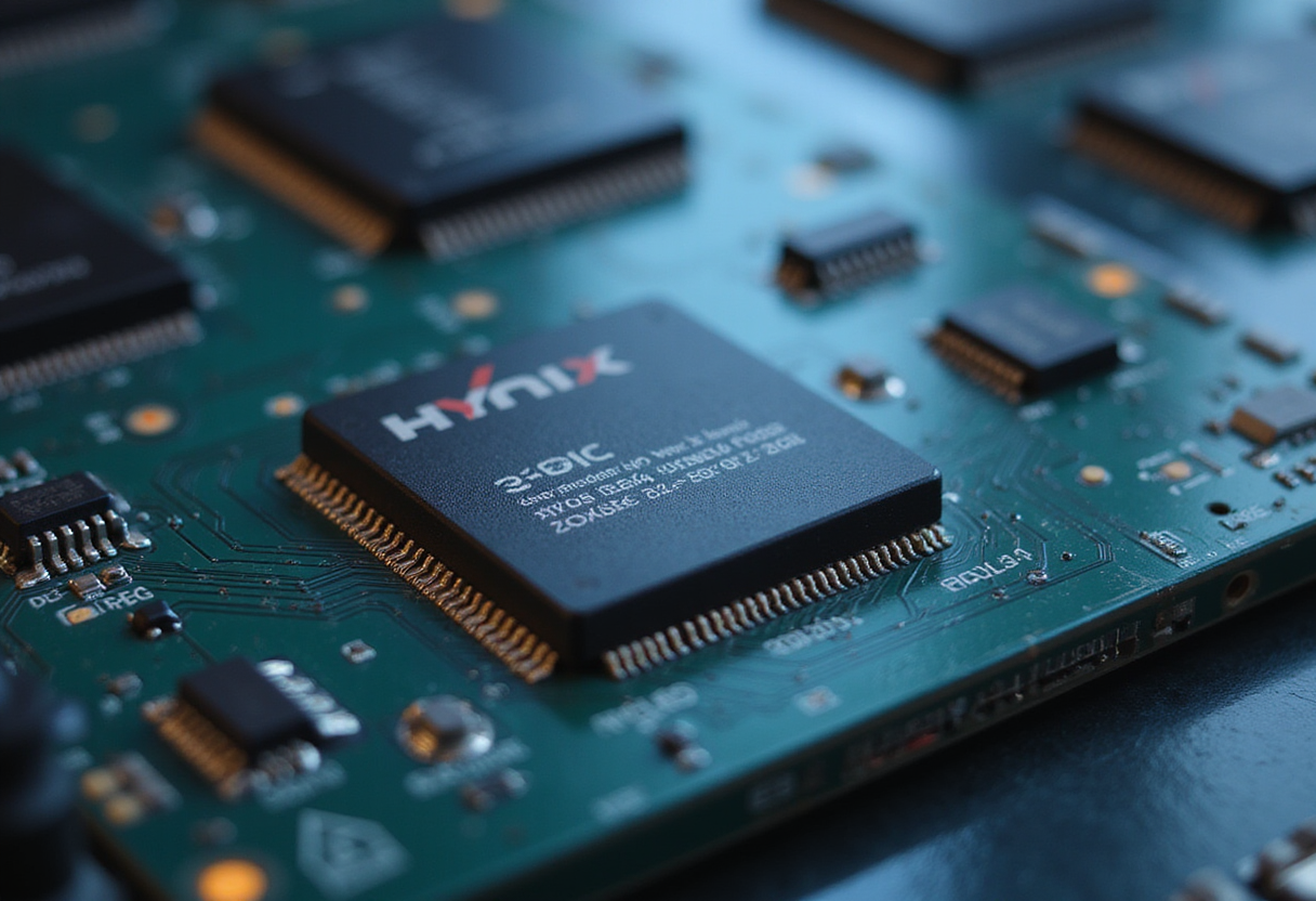
SK hynix has built a tiny in-house processor core — the Hynix Transaction Processing Unit, or H-TPU — that draws about 2.5% of a general-purpose CPU core's power while occupying roughly 4% of its area. The company plans to seed the cores across its NAND portfolio, including next-generation enterprise SSD controllers, according to a report from TheElec.
Not to be confused with a tensor processor for AI, the H-TPU targets the repetitive grunt work inside an SSD: read and write command processing, metadata management, and buffer control. It runs a four-stage, in-order pipeline. No superscalar units. No out-of-order execution. Clusters of these cores, more than 100 in total across dozens of small TPU clusters, handle routine I/O while a traditional Arm CPU keeps error recovery, exception handling, and storage-policy management to itself.
Why did SK hynix design its own core?
Koo In-jae, SK hynix's VP of SoC design, laid out the problem at ISOCC 2026, the International SoC Design Conference, in a talk titled "From SSD Controllers to AI Memory SoCs." SSD controller CPUs, he said, are at their limit on power and area. PCIe bandwidth doubles every generation, and controller CPU clocks and control capability reportedly can't keep up.
The industry's default answer has been to add cores. Marvell's PCIe 6.0 Bravera SC6 carries 12 Cortex-R82 cores in two six-core clusters, plus three Cortex-M7 cores and a secure Cortex-M3. Its PCIe 5.0 predecessor, the Bravera SC5, listed 10 Cortex-R8 and Cortex-M7 cores plus a Cortex-M3. Core counts have climbed with PCIe speeds out of necessity, and SK hynix's split treats that trajectory as a dead end. Storage control demands more than 100 detailed functions, which suits small single-job cores far better than one monolithic CPU. Cores a given I/O doesn't need idle in a minimum-power mode. SK hynix ships a dedicated compiler and development tools for the cores, which distinguishes them from fixed hardware macros.
Is the approach entirely new?
No. Phison's CoXProcessor has paired Cortex-R5 cores with hardened macros to offload repetitive firmware at wire speed for some time. Phison's E18 controller uses two lower-clocked Cortex-R5 cores to supplement three main ones, and its enterprise X1 paired two Cortex-R5 cores with up to 32 "micro cores," each dedicated to one or two tasks. H-TPU scales that idea up.
SK hynix's own patents sketch the architecture. U.S. patent 11,675,537, first filed in Korea in November 2020, describes a CPU-run control plane and an I/O plane of many small processors sorted into four groups — host, cache, map, and NVM — through which each command passes in order. In the patent's example, each small core runs about "200,000 logic gates" against the CPU's "seven million logic gates," or about 2.9% of the gate count, and "firmware may be driven in each of the TPUs," keeping the design adaptable.
What comes next — and where does it ship first?
The next step is hardware automation, or HWA: command processing, address lookup, and buffer copies move to dedicated circuits, while the CPU and H-TPUs keep exceptions and policy decisions. SK hynix filed on fixed-hardware paths back in 2014 through its San Jose-based unit, and later with U.S. patent 12,216,914, first filed in Korea in 2022, which describes a "write automation circuit" and says "a task without intelligent control can be handled or processed through the hardware layer."
The H-TPU is reportedly in use in "Storage Next," Nvidia's name for the joint AIN P project with SK hynix, targeting 512-byte or more limited NAND access. SK hynix also plans to apply it to high-bandwidth flash, due next year. HBF stacks NAND dies for AI inference, aiming at HBM-level bandwidth with up to 512GB per stack versus 64GB for HBM4. In HBF workloads, AI inference reads outnumber writes roughly 300,000 to 1, and the AI compiler and runtime pass pre-analyzed dataflow to the SoC so buffer management and prefetching can hide NAND latency behind compute. Space is tight in those stacks, which makes a traditional multi-core Arm design less practical.
H-TPU hasn't yet been proven in a shipping enterprise SSD controller, and no date has been given. With simple core scaling already suboptimal at current PCIe speeds, and PCIe 8.0 headed for final ratification in 2028, controller vendors will need designs like this long before the bandwidth doubling stops.
Source: Tom's Hardware
More from Rebecca Stone
Show full bio
Correspondent covering technology and product news in Semiconductors, chip manufacturing, hardware, AI compute at Chip Dispatch.
476 articles
Related articles
fractile-ceo-ai-bottleneck-is-memory-bandwidth-not-compute-d458a481
Fractile CEO: AI Bottleneck Is Memory Bandwidth, Not Compute
sk-hynix-says-solidigm-listing-not-yet-decided-995f494c
SK hynix Says Solidigm Listing Not Yet Decided
asus-ai-superbuild-puts-local-llms-on-a-172-tops-mini-pc-ef10affc
ASUS AI SuperBuild Puts Local LLMs on a 172-TOPS Mini-PC
sk-hynix-validates-hbm5-with-tsmc-retains-partner-of-the-year-457478f7
SK hynix Validates HBM5 with TSMC, Retains Partner of the Year