TSMC A14 reportedly revives SRAM scaling below 0.017 µm²
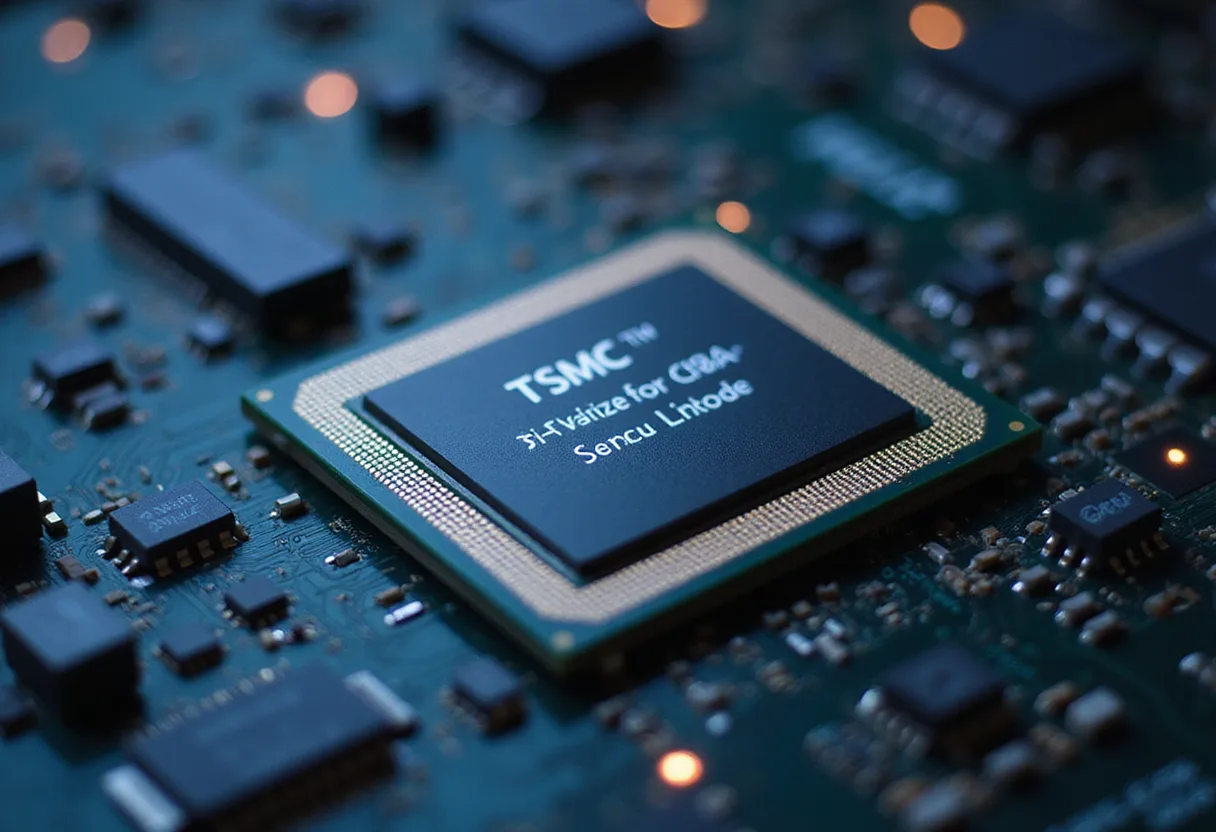
ETNews reports that TSMC's A14 will cut SRAM cells below 0.017 µm², more than 20% smaller than recent nodes, while targeting roughly 20% higher chip density.
- By
- Nathan Brooks
- Filed
- Channel
- Chip Manufacturing
- Read
- 3 min read
By Nathan Brooks
ETNews reports that TSMC plans to cut SRAM bit-cell area to below 0.017 µm² at its A14 node, a reported 20% SRAM scaling improvement over N2. The proposed cell would also be more than 20% smaller than the roughly 0.021 µm² used at 5 nm, 3 nm and 2 nm.
If that specification holds, TSMC would end a scaling pause that has lasted years. The commercial importance is greater than the usual node-label arithmetic. Logic transistors kept shrinking, but recent SRAM cells barely moved, leaving cache as an increasingly large share of new CPU and GPU dies.
What changes at A14?
ETNews attributes the sub-0.017 µm² figure to TSMC's plans, rather than to a disclosed production result. The report says TSMC will unveil the advancement later this year. Until formal specifications and measured data appear, the SRAM number remains a roadmap claim.
TSMC says its A14 process targets are:
- “A 10-15% speed improvement over N2 at the same power levels.”
- “A 25-30% power reduction at the same performance levels.”
- An approximately 20% increase in chip density.
These are development goals, not demonstrated results from shipping processors or other products made at A14. The distinction is commercially material. The SRAM-area claim and the broader density target remain separate measures: one describes a specific memory cell, while the other covers overall chip density.
Where TSMC could gain an edge
ETNews argues that the reported SRAM reduction would place TSMC ahead of Samsung and Intel. The report assesses that the rivals are unlikely to announce smaller SRAM cell sizes with their competing 14-Angstrom technologies. That is a forward-looking comparison, not a disclosed production result from either rival.
The advantage would have two commercial forms. A chipmaker could hold cache capacity constant, reduce the cache's physical area and lower the chip's cost. Alternatively, the company could keep the die size unchanged and use the recovered space for more on-chip cache.
For a fixed CPU or GPU footprint, that is the useful comparison: more cache in the same area, or the same cache in less area. Neither benefit yet has a measured cost impact in the report.
AMD has worked around the SRAM constraint by using 3D die stacking to boost cache capacity in its X3D gaming CPUs. A14 would offer a different route by shrinking the cells themselves. If A14 delivers the reported geometry, designers would have another route to cost reduction or cache growth.
Why SRAM scaling matters
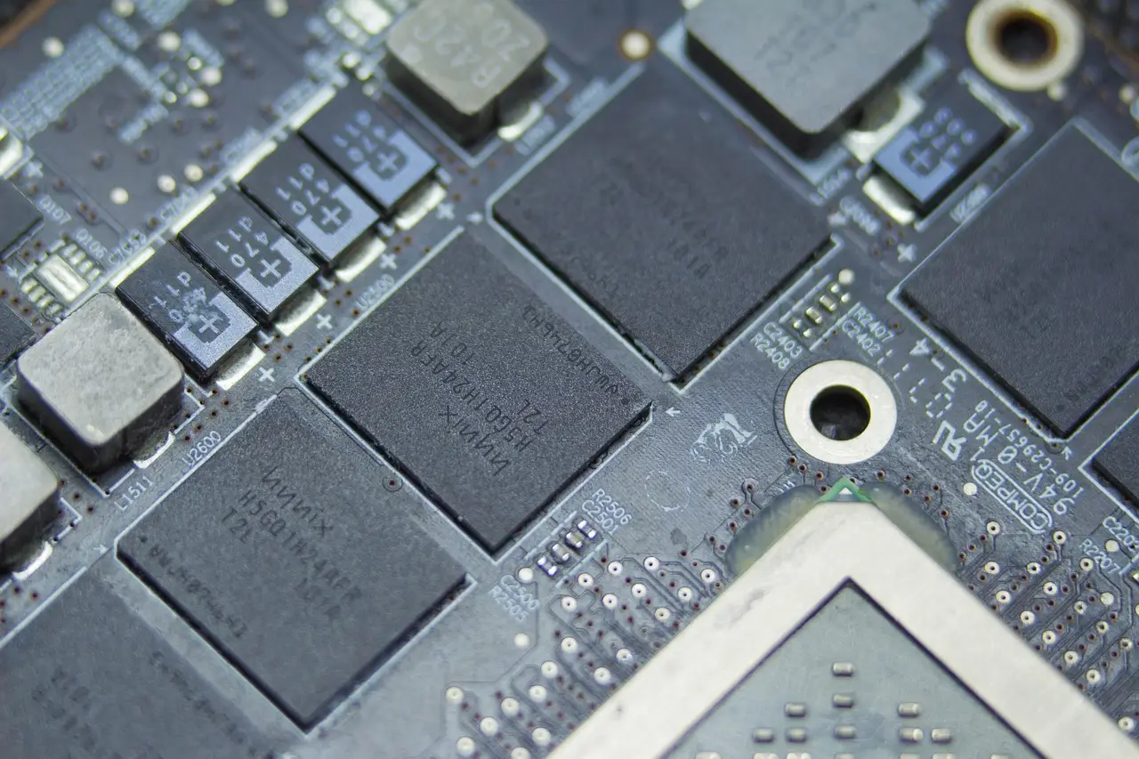
The mismatch between logic and SRAM scaling has changed processor economics. Because logic continued to shrink while SRAM remained around 0.021 µm², caches now occupy a larger proportion of advanced CPU and GPU dies. Large caches cost more to include, and they make processors with still greater cache capacity harder to produce.
Memory performance and bandwidth have also become increasingly severe bottlenecks for modern chips. Larger on-chip caches can partly counter those constraints, which makes restored SRAM scaling commercially relevant beyond a tidy node comparison.
ETNews therefore presents SRAM scaling as a potentially critical feature of A14 and a factor in TSMC's continued leadership in silicon manufacturing. The logic is straightforward: a smaller bit cell lowers the area burden of cache, while added cache can reduce pressure on memory bandwidth.
Still, A14's roughly 20% density target does not guarantee a 20% increase in cache capacity. Actual cache gains depend on the reported cell-area change and how chipmakers allocate the recovered die area, not on the density target alone.
If TSMC confirms the sub-0.017 µm² cell area when it unveils the advance later this year, A14's commercial case will rest on lower chip pricing or more cache per die, while Samsung and Intel still have room to answer through their competing 14-Angstrom options.
Source: Google News: TSMC
More from Nathan Brooks
Show full bio
Senior reporter covering people, launches and day-to-day practice in Semiconductors, chip manufacturing, hardware, AI compute at Chip Dispatch.
740 articles
Related articles
tsmc-targets-1-4nm-mass-production-in-h1-as-apple-lines-up-88c17a84
TSMC Targets 1.4nm Mass Production in H1 2028 as Apple Lines Up
tsmc-and-apple-target-1-4nm-chips-as-costs-climb-f6dfa236
TSMC and Apple Target 1.4nm Chips by 2028 as Costs Climb
tsmc-s-a14-node-draws-customer-interest-ahead-volume-production-ff6031cc
TSMC's A14 Node Draws Customer Interest Ahead of 2028 Volume Production
tsmc-expands-2nm-capacity-as-apple-and-nvidia-orders-climb-92bb33ee
TSMC Expands 2nm Capacity as Apple and Nvidia Orders Climb