AI-Designed Silicon Cavities Lift Atom-Thin Emitter Output Tenfold
AI-designed silicon cavities reportedly lift light emission tenfold from an atom-thin semiconductor, though the summary names no baseline, material, or publication venue.
- By
- Sophie Lindqvist
- Filed
- Channel
- Semiconductors
- Read
- 3 min read
By Sophie Lindqvist
A tenfold increase in light emission from an atom-thin semiconductor has been reported, using silicon optical cavities designed by artificial intelligence. The claim comes from a research summary carried by Bioengineer.org. The headline figure is a multiplier, not a milliwatt count. That distinction matters.
The source names no absolute output power, no quantum efficiency, and no wavelength. A tenfold relative gain over an unspecified baseline leaves the practical significance open. Readers should hold the number accordingly.
What is actually claimed?
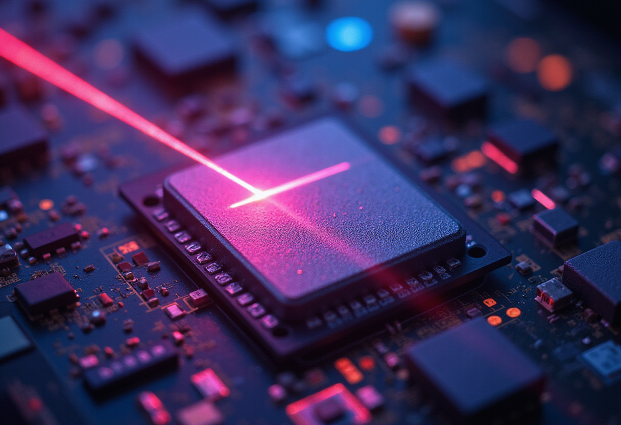
The reported mechanism is straightforward. Researchers placed a two-dimensional semiconductor — a material one atomic layer thick — inside silicon cavities whose geometry an AI system designed. The cavities confine light near the emitter. Better confinement means more of the generated photons escape usefully instead of being lost.
Silicon is the substrate of the entire logic industry. Pairing it with a 2D emitter points at integrated photonics, where on-chip lasers and light sources remain a hard problem. Silicon itself emits light poorly. A 2D material supplying the emission, with silicon supplying the cavity, is a plausible division of labor.
That is the plausible part. The confirmation part is thinner.
What the report does not say
The published summary, as surfaced, gives only the headline result. Several items are absent:
- No institution or laboratory is named in the available text.
- No journal, publication date, or peer-review status appears.
- The specific 2D material is not identified. Candidates range from tungsten diselenide to molybdenum disulfide, and their properties differ.
- The AI method is not described. "Designed by AI" can mean brute-force optimization, inverse design, or a trained surrogate model.
- No comparison against cavities designed by conventional methods is stated. Without it, the AI contribution cannot be separated from the cavity contribution.
Each gap is normal for a press digest. Each gap also weakens the claim's verifiability at this stage. A tenfold gain achieved by AI design would be more persuasive with a control arm designed by humans.
Why the direction matters anyway
Integrated photonics is a real commercial frontier. Optical interconnects already carry traffic between and inside data centers. Co-packaged optics are moving into switches. The industry wants light sources built directly on silicon, at CMOS-compatible temperatures and costs.
2D semiconductors hold a structural advantage here. They can sit on silicon without the lattice-matching constraints that make conventional III-V laser epitaxy on silicon difficult and expensive. Strain and defects limit direct growth of gallium arsenide or indium phosphide on silicon wafers. A material that is one layer thick largely sidesteps that problem.
Cavity design then becomes the bottleneck. Inverse design tools, often AI-driven, search geometries that human intuition would not try. If such a tool genuinely delivered a 10x emission gain here, it supports a broader trend: computational design substituting for fabrication complexity.
How to read the tenfold figure
Relative gains shrink when the baseline is weak. A poorly emitting unpatterned film leaves large headroom; a well-optimized structure does not. The report does not state the baseline. It does not state whether the gain holds across wavelengths, temperatures, or device lifetimes. None of these caveats refute the result. They define the distance between a laboratory demonstration and a manufacturable component.
Silicon cavities carry one more advantage the headline implies. They are fabricable in standard processes. A result that depends on exotic patterning would carry less industrial weight. If the cavities used here are CMOS-compatible, the path to scale-up shortens considerably — but the source does not confirm that either.
What to watch next
The claims will face scrutiny at the level where such results live or die: peer-reviewed publication with full methods, absolute emission figures, and a conventional-design control. Confirmation would strengthen the case for AI-designed photonics as a practical design tool rather than a laboratory curiosity. Until then, the tenfold number stands as a reported result, promising but unverified.
Source: Google News: semiconductors
More from Sophie Lindqvist
Show full bio
News editor covering money, funding and market shifts around Semiconductors, chip manufacturing, hardware, AI compute at Chip Dispatch.
389 articles
Related articles
laser-written-glass-chip-hits-42-7-gbit-s-quantum-randomness-e4e8c165
Laser-Written Glass Chip Hits 42.7 Gbit/s Quantum Randomness
caltech-prints-fiber-grade-optics-on-8-and-12-inch-silicon-wafers-787f0d35
Caltech Prints Fiber-Grade Optics on 8- and 12-Inch Silicon Wafers
vexlum-raises-10-million-to-scale-semiconductor-laser-output-0e815165
Vexlum Raises €10 Million to Scale Semiconductor Laser Output
uc-davis-shrinks-ai-spectrometer-chip-to-0-4-mm2-on-plain-silicon-0f0bf179
UC Davis Shrinks AI Spectrometer Chip to 0.4 mm² on Plain Silicon