Ex-Microsoft Engineer Builds PDP-11 RAM Board on FPGA With AI Help
Dave Plummer paired a Lattice MachXO2 FPGA with four ISSI 1 MB chips to replace unaffordable PDP-11 memory — then hit a byte-lane bug that halved capacity.
- By
- Sophie Lindqvist
- Filed
- Channel
- Hardware & Components
- Read
- 4 min read
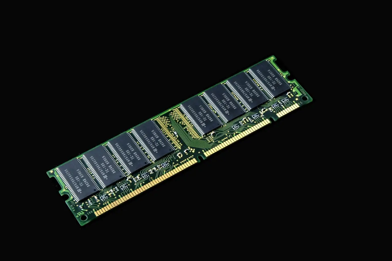
Four megabytes of original PDP-11 memory costs more than most used cars, so Dave Plummer built his own RAM board instead. Plummer is the former Microsoft engineer best known for Task Manager and Windows Pinball. After counting the zeros on the price tag for a megabyte of memory for his vintage PDP-11, he decided the commercial route made no economic sense and designed a replacement himself.
The PDP-11 dates from 1970. Later models supported up to four megabytes of memory. That ceiling set Plummer's target for the board.
What hardware did he actually build?
Plummer designed the RAM as a standalone Q-Bus card, the bus format several PDP-11 models use for main system components. He tested it on a backplane next to another board holding the system's M8190 CPU. He acknowledged up front that he had never done a project of this complexity before.
The parts list is short and specific:
- A Lattice MachXO2 FPGA, model 2000HC, serving as the memory controller
- Four ISSI 1 MB memory chips
- A U2S I/O chip
- A bank of DIP switches, comm ports, and a handful of capacitors
The M8190 board design uses a 22-bit bus and reserves the top 256 KB for I/O and ROM. Plummer credits two tools for getting him through the design: ChatGPT and the EasyEDA online circuit simulator. The claim is his own, and there is no independent verification of how much the AI actually contributed.
Where did the project go wrong?
It was not a first-try success. Plummer had never flash-programmed an FPGA before and needed several attempts before that step worked. Then he hit what appears to be a classic PDP-11 trap, one that the source does not say he anticipated.
The machine's memory bus design accesses entire words — two bytes — at once. The lowest bit in a memory address acts as a lane selector between the low and high byte within the word. On reads, the CPU picks out the correct byte itself, but the memory controller must still return both. On writes, the controller must read the existing word, swap in only the selected byte, and write back the full word. Otherwise the bus lines carry an entire word that can overwrite valid data with invalid data.
Plummer, by his own account, did not know this in advance. One commenter joked that he had "built 4MB of memory that turned out to be 2MB." Plummer replied that the memory "only returns every second word" — a direct confirmation that the bug matched the known design pattern, not a denial.
The source offers no follow-up update. Other commenters pointed out the same flaw, and the article's author assumes an easy fix in the FPGA code followed. That assumption is unconfirmed. No revised design, test result, or working demonstration appears in the material.
Is an FPGA even the right approach?
One commenter proposed sidestepping the hardware problem entirely: implement the memory in software on a Raspberry Pi wired directly to the PDP bus. Plummer answered that he had effectively done that already the previous week. His setup used a modern QBone DEC interface board, which carries a Beaglebone Black — a board in the same class as a Raspberry Pi — mounted atop it.
So the FPGA board is not his first attempt at solving the memory problem. It is the second approach, following a working software-based path. The source does not say which solution he considers final, or whether the FPGA board will be repaired at all.
What does this say about AI-assisted hardware design?
The story carries a familiar promise: an engineer with no prior FPGA experience ships a working memory controller with AI assistance. The caveats deserve equal weight. The first version shipped with a byte-addressing bug that halved effective capacity. The fix is assumed, not demonstrated. And Plummer had already reached the same goal with an off-the-shelf QBone and Beaglebone Black. If the FPGA board reaches full, verified 4 MB operation, it will be a genuine piece of reverse-engineering. Until he publishes a corrected design, the working memory in that PDP-11 remains the software version.
Source: Tom's Hardware
More from Sophie Lindqvist
Show full bio
News editor covering money, funding and market shifts around Semiconductors, chip manufacturing, hardware, AI compute at Chip Dispatch.
742 articles
Related articles
d-matrix-tapes-out-raptor-xpu-targets-10x-hbm4-bandwidth-364c686f
d-Matrix Tapes Out Raptor XPU, Targets 10x HBM4 Bandwidth
goldman-names-three-stocks-to-ride-high-performance-nand-s-ai-surge-c9c7c8ca
Goldman names three stocks to ride high-performance NAND's AI surge
micron-lines-up-512gb-ddr5-rdimm-for-12tb-servers-in-h2-e0f48421
Micron Lines Up 512GB DDR5 RDIMM For 12TB Servers In H2 2027
micron-aims-eim-memory-chip-mass-production-115a8dca
Micron Aims EIM Memory Chip at 2028 Mass Production