Hamamatsu Launches iPHEMOS-DDX Inverted Emission Microscope
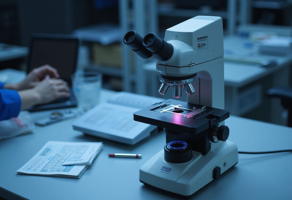
Hamamatsu Photonics introduces the iPHEMOS-DDX inverted emission microscope, aimed at failure analysis of advanced semiconductor packages with stacked, chiplet-based architectures.
- By
- Tom Whitfield
- Filed
- Channel
- Chip Manufacturing
- Read
- 3 min read
Hamamatsu Photonics has introduced the iPHEMOS-DDX, an inverted emission microscope built for failure analysis of advanced semiconductor packages. The company announced the product through a PR Newswire release, positioning it as an addition to its long-standing iPHEMOS family of emission microscopy tools used in semiconductor defect inspection.
The launch targets one of the more persistent bottlenecks in chip manufacturing: localizing faults in packages whose density and stacked architecture keep climbing. As fabs and OSATs move to advanced packaging formats — chiplets, multi-die stacks and high-density interposers — traditional front-side inspection reaches its limits, and failure analysis teams need instruments that can approach the device from the substrate side.
That is the gap the inverted optical configuration of the iPHEMOS-DDX addresses. By imaging from below, the instrument can reach failure sites in flip-chip and otherwise obscured package structures that a conventional upright emission microscope cannot observe directly.
What does the new tool change?
Emission microscopy works by detecting the faint photons that leak from a defective transistor junction, interconnect or dielectric when the device is electrically stressed. Localization of that photoemission pinpoints where physical analysis — cross-sectioning, FIB milling, electron microscopy — should follow. The faster and more precisely that hotspot is found, the shorter the failure-analysis loop and the quicker a yield problem or field return is understood.
Advanced packages complicate this loop in a specific way: the emission site sits under solder bumps, underfills and substrates rather than under a transparent backside or an open die surface. An inverted stage brings the objective lens to the emission path from the package side, which is where Hamamatsu has aimed the DDX design.
For failure-analysis labs at logic foundries, memory makers, OSATs and IDM reliability groups, the tool category is not optional. Every advanced-node product and every 2.5D or 3D package that goes into automotive, AI-accelerator or mobile silicon passes through emission-based fault isolation at some point in debug and qualification.
Why packaging is pulling failure analysis tooling
The commercial context is straightforward. Advanced packaging has moved from a back-end specialty to a primary vector of product differentiation, and analysis equipment vendors are following the inspection problem to where it now lives: in the stack, not just on the die.
Hamamatsu Photonics, headquartered in Hamamatsu City, Japan, is one of the established suppliers of photonics-based measurement and analysis instruments, with the iPHEMOS line among the recognizable names in emission microscopy for semiconductor failure analysis. Extending that line toward inverted configurations signals where the company expects demand to concentrate as package complexity rises.
What comes next
Full specifications, availability and pricing for the iPHEMOS-DDX were not part of the announcement summary; Hamamatsu will publish that detail through its standard product channels. If adoption follows the trajectory of advanced packaging itself, expect inverted emission microscopy to become a routine fixture in failure-analysis labs handling multi-die products over the coming device generations.
Readers should treat capability claims as vendor statements until independent lab evaluations appear.
Source: Google News: semiconductors
More from Tom Whitfield
Show full bio
Staff writer covering consumer brands and retail at Chip Dispatch.
269 articles
Related articles
hamamatsu-packs-seven-failure-analysis-modes-into-iphemos-ddx-microscope-732d5e0a
Hamamatsu Packs Seven Failure-Analysis Modes Into iPHEMOS-DDX Microscope
chip-inspection-equipment-makers-see-valuations-climb-e163096e
Chip Inspection Equipment Makers See Valuations Climb
makr-microsystems-raises-rs-10-2-crore-for-chip-inspection-tech-db35b631
Makr Microsystems Raises Rs 10.2 Crore for Chip Inspection Tech
shindo-eng-lab-pivots-from-display-tools-into-chip-packaging-56d176dd
Shindo Eng. Lab Pivots From Display Tools Into Chip Packaging