Japan, US in Talks to Build US Chip Factory as Part of Tariff Deal
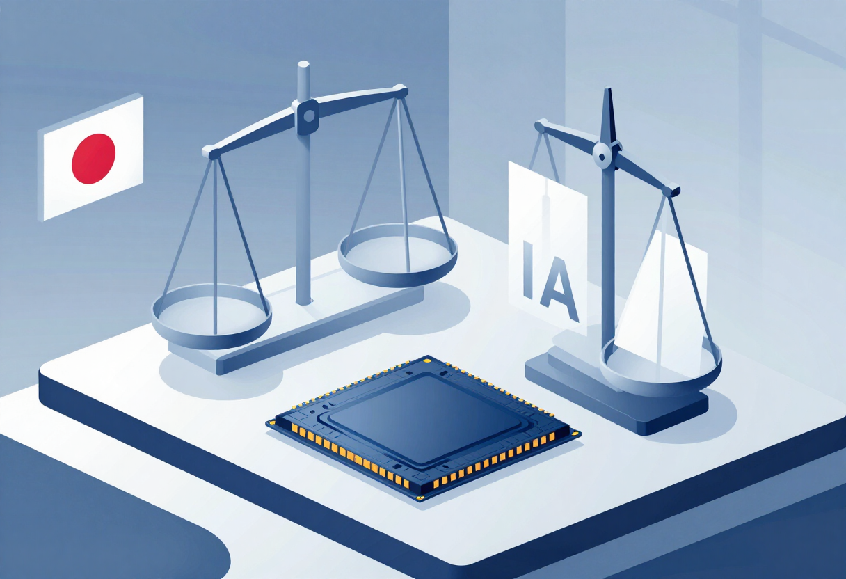
Japan and the United States are negotiating a US semiconductor fab as part of a tariff deal, Nikkei Asia reported. The disclosure names no operator, node, capacity, site or investment total.
- By
- Grace Kim
- Filed
- Channel
- Chips & Policy
- Read
- 3 min read
Japan and the United States are negotiating the construction of a US-based semiconductor fabrication plant as part of a tariff deal, Nikkei Asia reported. The headline-level disclosure carries no identified operator, process node, wafer size, capacity target, or investment total.
What does the headline confirm?
The Nikkei report supplies three concrete elements. First, two-party talks are underway between the governments of Japan and the United States. Second, the subject of those talks is a chip factory sited on US soil. Third, the project sits inside a tariff-deal framework rather than standing alone.
No direct quotations from named officials appear in the available material. The headline credits no corporate source, government spokesperson, or diplomatic readout. The story circulated only as a title and URL through aggregator channels.
What details are still undisclosed?
Several categories of operating detail are absent from the source. The fab operator goes unnamed. The headline leaves the process technology unspecified, leaving open whether the plant would target a leading-edge node such as 2 nm or 3 nm, a trailing-edge node for automotive or industrial parts, or a specialty technology for analog, power, or MEMS devices.
Capacity also goes unstated. Comparable US fabs now under construction have disclosed ranges from roughly 50,000 to 100,000 wafer starts per month, depending on the operator and node. Mature nodes sometimes exceed that range at single sites, particularly for automotive microcontrollers. The source provides no figure to anchor any comparison.
Project cost similarly goes undisclosed. Comparable greenfield US semiconductor projects have absorbed tens of billions of dollars in committed capital, with public commitments ranging from roughly $10 billion for incremental expansions to more than $40 billion for new leading-edge campuses. Without a Nikkei-reported total, no dollar benchmark can be drawn from the headline.
Site selection also goes undisclosed. Wafer fabs typically demand large flat sites, abundant water supply, stable electricity, and proximity to back-end packaging and test infrastructure. Post-announcement site selection usually spans 12 to 24 months on those criteria.
How does the tariff component fit the proposal?
The headline places the fab proposal inside a tariff package. Linking investment commitments to trade negotiations has become a recurring feature of Washington's recent dealings with allied governments, a structure that converts duty adjustments into capital pledges and procurement targets.
A factory announcement tied to the tariff package would deliver a tangible industrial-policy outcome from a broader trade framework, shifting the conversation from abstract commitments to shovel-ready capital deployment. Such announcements typically translate into construction milestones measured in years, not quarters.
The disclosure does not specify whether the fab substitutes for, supplements, or accompanies broader tariff concessions. Each structure carries different implications for chip supply chains and downstream electronics pricing in the years that follow groundbreaking.
What signal should watchers expect next?
The next public signal will likely arrive as a coordinated joint statement, a named operator disclosure, or a regulatory filing tied to site acquisition. Until then, the proposal remains an unconfirmed framework item under active negotiation.
Watchers can also expect clarifying readouts from individual ministries as the underlying tariff schedule takes shape. Each subsequent disclosure will likely narrow the operational details surrounding any new US-based Japanese-linked fab, beginning with the operator's identity and the node targeted for production. Pricing dynamics on established advanced-node memory and logic products, along with capacity availability across both leading-edge and trailing-edge nodes, will frame the commercial significance of the eventual project.
By Grace Kim, Senior Editor
Source: Google News: chip factory investment
More from Grace Kim
Show full bio
Market editor covering people, launches and day-to-day practice in Semiconductors, chip manufacturing, hardware, AI compute at Chip Dispatch.
364 articles
Related articles
japan-and-us-in-talks-over-chip-fab-under-550-billion-investment-plan-a855977a
Japan and US in Talks Over Chip Fab Under $550 Billion Investment Plan
japan-and-us-weigh-19-billion-chip-plant-in-tariff-investment-pact-8dcdcf17
Japan and US Weigh $19 Billion Chip Plant in Tariff Investment Pact
japan-us-weigh-chip-fab-buildout-inside-550b-investment-framework-10bde8b1
Japan, US weigh chip fab buildout inside $550B investment framework
tsmc-s-u-s-investment-commitment-rises-to-265-billion-a63c22d6
TSMC's U.S. Investment Commitment Rises to $265 Billion