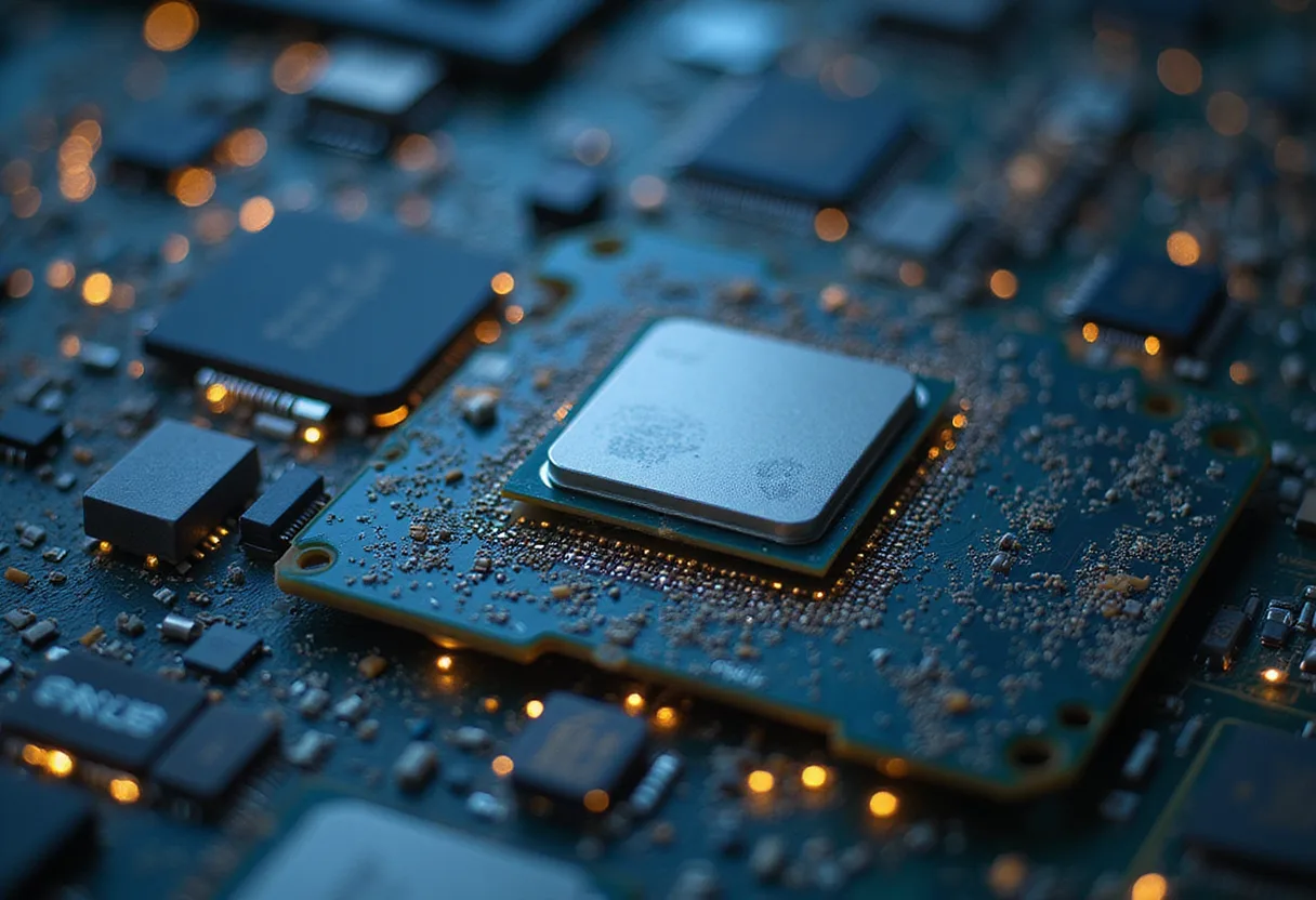
Leaked Nova Lake Die Shots Show Six-Tile Design on Intel 18A-P and TSMC N2P
Leaked die shots of Intel's Nova Lake reveal a modular six-tile layout that reportedly pairs Intel 18A-P compute tiles with TSMC N2P silicon from external foundries.
- By
- Tom Whitfield
- Filed
- Channel
- Chip Manufacturing
- Read
- 4 min read
Leaked die shots published by TweakTown appear to show Intel's Nova Lake client processor built from six separate tiles, with compute silicon on Intel's 18A-P process and other tiles reportedly fabbed by TSMC on its N2P node. If the images are genuine, Nova Lake becomes the clearest example yet of Intel's plan to mix its own leading-edge manufacturing with external foundry supply inside a single product family.
The leak, which TweakTown attributes to die-shot analysis of early Nova Lake silicon, describes a modular topology rather than a monolithic die. Six tiles sit in one package. The arrangement follows the disaggregated design philosophy Intel introduced with Meteor Lake, where the company splits compute, graphics, input-output and platform functions into separate chiplets and connects them through an interconnect fabric.
What do the die shots actually show?
According to TweakTown's report, the key detail is the split in manufacturing sources. The compute tiles — the cores that do the heavy lifting — sit on Intel 18A-P, the performance variant of Intel's 1.8-nanometer-class node. Other tiles in the package reportedly come from TSMC on N2P, the enhanced second generation of TSMC's 2-nanometer family.
This matters because it confirms, at die level, what industry observers have long suspected about Intel's client roadmap. Intel has said since 2021, when CEO Pat Gelsinger launched the IDM 2.0 strategy, that roughly 20 to 30 percent of its products could use external foundries. Nova Lake appears to push that share toward the upper end for at least one mainstream client generation.
The picture is a leak, not a product announcement. Intel has not confirmed the die shots, the tile count or the process split, and specifications can change before production parts ship. Everything beyond the images themselves — yields, volumes, launch timing, SKU structure — remains outside the confirmed record.
Why does a dual-foundry design matter commercially?
The commercial logic runs through cost and capacity. Compute tiles are the most performance-sensitive silicon, and keeping them on Intel 18A-P preserves the company's claim that its most advanced node powers its most important product. Moving graphics, I/O or SoC-class tiles to TSMC N2P lets Intel buy proven capacity where it does not need to lead on transistor density.
For TSMC, the deal would extend a relationship that already covers Intel's graphics tiles in Meteor Lake and Lunar Lake-class products. N2P is positioned as a refined version of N2, offering density and efficiency improvements over the base node. A multi-tile Nova Lake order would give TSMC a second major Intel product line on its 2-nanometer generation.
The geopolitical context is real but secondary here. A single package that draws on fabs in both the United States and Taiwan diversifies supply risk at the component level. What changes the commercial picture is pricing: dual-sourced tiles give Intel a second cost benchmark against its internal Foundry unit, which is exactly the internal-market discipline Intel's board has demanded since the foundry business began reporting standalone losses.
How does this fit the roadmap?
Nova Lake is the client generation Intel has placed after Arrow Lake in its public sequencing, and the leaks suggest it will lean harder into tile modularity than any Intel client chip before it. Six tiles would exceed the four-tile layout of Meteor Lake and points toward a platform where Intel can scale core counts and features by adding or removing tiles rather than redesigning a monolithic die.
The competitive target is plain. AMD already ships chiplet-based client processors on TSMC nodes, and Apple moves monolithic designs through TSMC's leading edge on annual cadence. A six-tile Nova Lake on 18A-P plus N2P would put Intel's silicon strategy somewhere between the two — internal leading-edge compute, external leading-edge everything else.
Until Intel confirms the design at a formal event, the die shots remain a leak with strong internal consistency but no official standing. The takeaway in plain words: if these images hold up, Intel's next flagship client processor will be built as much from TSMC wafers as from its own, and that balance will shape pricing and capacity decisions across both foundries through 2026 and beyond.
Source: Google News: TSMC
More from Tom Whitfield
Show full bio
Staff writer covering companies, deals and strategy in Semiconductors, chip manufacturing, hardware, AI compute at Chip Dispatch.
585 articles
Related articles
panther-lake-teardown-puts-intel-18a-under-the-microscope-0ed3066f
Panther Lake Teardown Puts Intel 18A Under the Microscope
panther-lake-teardown-intel-18a-lands-near-tsmc-n3e-abc6fa43
Panther Lake Teardown: Intel 18A Lands Near TSMC N3E
intel-s-14a-process-targets-tsmc-parity-foundry-margin-path-unclear-203bd58c
Intel's 14A Process Targets TSMC Parity; Foundry Margin Path Unclear
semianalysis-publishes-teardown-of-intel-s-panther-lake-silicon-2743a6ab
SemiAnalysis Publishes Teardown of Intel's Panther Lake Silicon