TSMC to Build 3nm Line at Second Japan Fab in $23 Billion-Plus Push
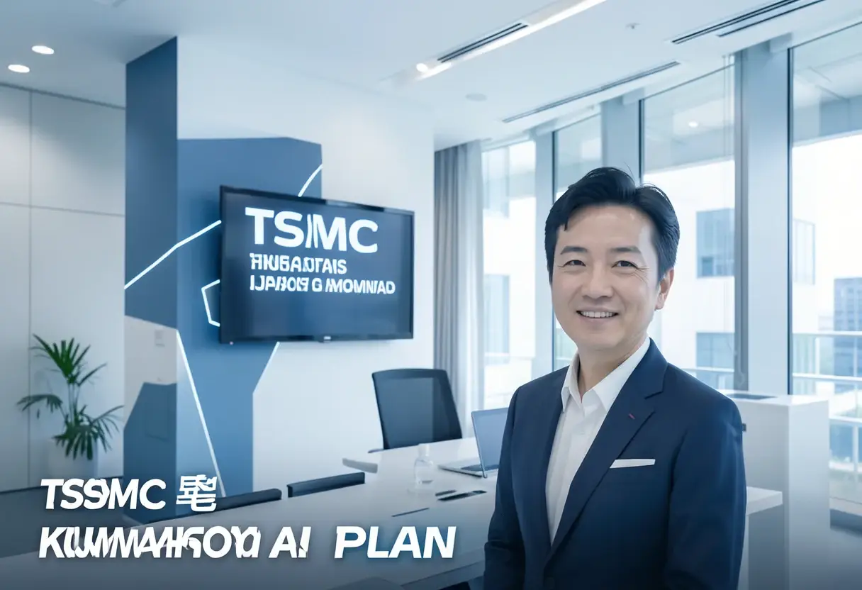
TSMC plans 3nm production at its second Kumamoto fab, with investment above USD 23 billion — its most advanced process placed outside Taiwan for the first time.
- By
- Sophie Lindqvist
- Filed
- Channel
- Chip Manufacturing
- Read
- 3 min read
TSMC will manufacture 3nm chips at its second factory in Japan, and total investment in the site will exceed USD 23 billion. That figure, reported by The Tribune, marks the largest single commitment TSMC has made to Japanese soil to date. It also pushes the Kumamoto complex firmly into advanced-node territory.
The number matters more than the announcement itself. TSMC's first Japanese fab, operated through its JASM subsidiary, was scoped for 12nm-class and older processes. A 3nm line at the second factory changes the character of the site. Japan would host leading-edge logic, not just mature specialty production for automotive and image sensors.
Caveats apply. The Tribune headline reports a plan, not a signed capacity target. TSMC has not, in this report, stated wafer output, production start dates, or how the USD 23 billion splits between the two phases. Investors should treat the figure as a stated investment intention until TSMC files updated capex guidance.
What does the 3nm move signal?
Process selection is the sharpest signal here. N3-family production currently sits in Taiwan, at TSMC's Hsinchu and Tainan fabs. Placing 3nm capability in Japan would represent the first leading-edge logic node TSMC builds outside Taiwan at scale.
The commercial logic is straightforward. Customers in Japan — particularly automotive and industrial semiconductor buyers — want geographically diversified supply. Tokyo wants domestic advanced logic capacity and has shown willingness to fund it. A 3nm line strengthens TSMC's pitch to Japanese customers who cannot wait on cross-border logistics.
What the report does not say is equally important. There is no word yet on customer commitments tied to the second fab, no monthly wafer capacity figure, and no confirmation of government subsidy amounts for this phase. Previous TSMC Japan subsidies required matching private investment, and that structure likely persists.
Why is the money figure a threshold?
Exceeding USD 23 billion places the Kumamoto expansion in the same weight class as TSMC's Arizona commitments. Advanced-node fabs cost roughly USD 15-20 billion each once cleanroom, tools, and support facilities are counted, so the figure implies more than a single modest line.
For Japan, the number is a policy statement. The government has committed substantial public funds to rebuilding domestic semiconductor manufacturing, and TSMC's Kumamoto site has been the flagship of that effort. A second factory at this scale extends the timeline of that bet well into the 2030s.
The caveat: investment announcements and operating fabs are different things. Tool installation, staffing, and qualification for a 3nm line each carry execution risk. TSMC's overseas projects have historically run slower than their Taiwan equivalents.
Who benefits, and who watches closely?
Renesas, Sony, and other JASM stakeholders gain from a deeper local ecosystem. Suppliers of extreme ultraviolet lithography support, chemicals, and wafers gain a larger anchor customer in Kyushu. The Tribune report does not name new partners, so any additions to the shareholder list remain unconfirmed.
The competitive pressure lands on Samsung Foundry and on Japan's own Rapidus. Samsung has trailed TSMC in advanced-node yield share for years. Rapidus, which targets 2nm-class production in Hokkaido, now faces a leading-edge competitor inside its home market, backed by the world's largest foundry.
Samsung has not commented on this specific expansion. Neither, per the report, has Rapidus.
What happens next?
Watch for three confirmations. TSMC must publish a construction timetable for the second fab. Tokyo must disclose the subsidy package attached to this phase. And the first named customers for the 3nm line will reveal whether demand is real or projected.
The Tribune gives the plan, the node, and the price. Until TSMC gives capacity and dates, the USD 23 billion figure is a promise with a number attached — and promises in this industry are measured in wafers shipped, not dollars pledged.
Source: Google News: TSMC
More from Sophie Lindqvist
Show full bio
News editor covering money, funding and market shifts around Semiconductors, chip manufacturing, hardware, AI compute at Chip Dispatch.
657 articles
Related articles
tsmc-to-bring-3nm-production-to-second-japan-fab-investment-above-23-billion-558f82ff
TSMC to Bring 3nm Production to Second Japan Fab, Investment Above $23 Billion
japan-clears-tsmc-3-nm-fab-plan-extending-kumamoto-build-out-b5603beb
Japan Clears TSMC 3 nm Fab Plan, Extending Kumamoto Build-Out
tsmc-s-3nm-kumamoto-plan-wins-japan-approval-up-to-4-1-billion-in-aid-52ab9940
TSMC's 3nm Kumamoto Plan Wins Japan Approval, Up to $4.1 Billion in Aid
tsmc-plans-another-3nm-fab-in-tainan-evertiq-reports-bb83a047
TSMC Plans Another 3nm Fab in Tainan, Evertiq Reports