Fujifilm Puts $18 Million Into US Slurry Capacity
Fujifilm will spend $18 million expanding US semiconductor slurry production — a small number that says much about where materials capacity is heading.
- By
- Nathan Brooks
- Filed
- Channel
- Chip Manufacturing
- Read
- 3 min read
Fujifilm will spend $18 million to expand production of semiconductor polishing slurry in the United States. The figure is small by fab standards and large by consumables standards. That asymmetry is the story.
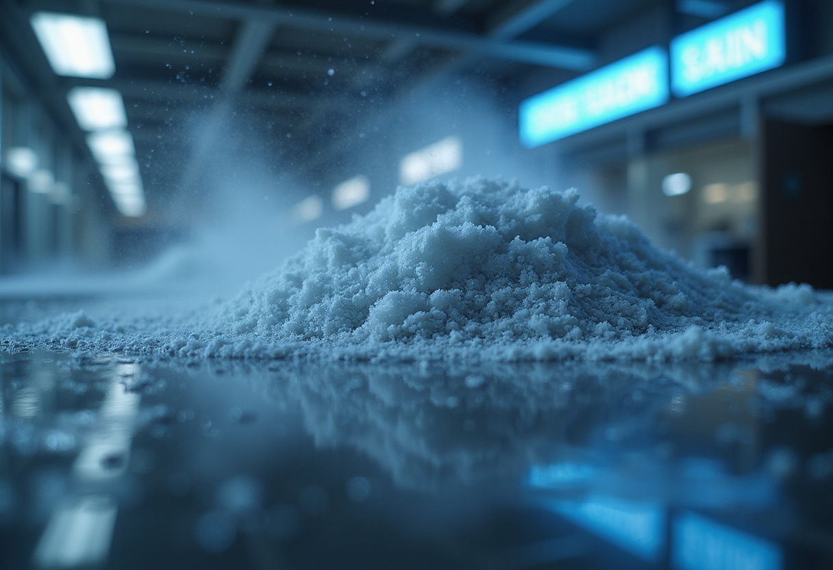
CMP slurry — the abrasive chemical mix used in chemical mechanical planarization — is unglamorous, low-margin compared with lithography tools, and utterly indispensable. No planarization, no working interconnect stack. Every wafer that passes through an advanced node consumes it by the barrel. Suppliers who ship it late, or from the wrong continent, stop a line just as effectively as a missing scanner.
An $18 million investment does not build a fab. It buys tanks, blending capacity, quality control, and proximity. For a consumables producer, that is the whole point: slurry is heavy, humidity-sensitive in handling, and expensive to ship across oceans. Local supply shortens logistics chains and insulates customers from freight shocks.
Why is a Japanese photo company making slurry?
Fujifilm's presence in semiconductor materials is not a pivot. It is the descendant of decades of film chemistry — colloids, coatings, particle control — that translate almost literally into polishing slurries and photoresists. The company supplies materials across the process chain and has spent recent years pushing that division's scale and geography.
The geography is the decision here. The United States is attracting both fab construction and the materials base that must sit within reach of those fabs. A slurry plant on US soil serves any domestic customer regardless of what happens to tariffs, export regimes, or Pacific shipping rates. Consumables follow capacity. That rule now works in America's favor.
What does $18 million actually buy?
In semiconductor capital terms, it buys a rounding error. A leading-edge fab costs a hundred times more. But slurry blending lines are not lithography machines, and the economics differ: incremental, modular, and demand-led. An $18 million expansion is a bet on existing US wafer volumes growing, not on a speculative greenfield.
It is also a hedge for Fujifilm's customers. Advanced packaging — which multiplies polishing steps per device — has been pulling slurry demand upward faster than front-end wafer growth alone would suggest. Chipmakers stacking dies need more planarization per unit of revenue. Suppliers who cannot scale blending capacity nearby will watch that demand go elsewhere.
Does this change the supply picture?
Not this quarter. Chemical capacity additions ramp slowly, with qualification cycles that stretch months as customers validate each lot against process windows. The expansion signals intent; volume follows on the materials industry's own clock.
The competitive read is simpler. Materials suppliers — Fujifilm among the largest in slurries, alongside rivals such as CMC Materials and Merck's electronics arm — are quietly repositioning assets toward where wafers will be processed rather than where they historically were. That shift costs each player millions, not billions. It is affordable, repeatable, and cumulative.
Fujifilm's $18 million will not make headlines beside multi-billion-dollar fab announcements. It will help determine whether those fabs run at full rate. Expect further materials investments of this size as US wafer capacity firms up — the quiet money moves first, and it usually knows something.
By Nathan Brooks, Chip Dispatch.
Source: Google News: semiconductors
More from Nathan Brooks
Show full bio
Senior reporter covering people, launches and day-to-day practice in Semiconductors, chip manufacturing, hardware, AI compute at Chip Dispatch.
516 articles
Related articles
fujifilm-to-showcase-u-s-manufacturing-at-semicon-west-2026-cc693358
Fujifilm to Showcase U.S. Manufacturing at SEMICON West 2026
fujifilm-commits-18-million-to-mesa-semiconductor-materials-expansion-5df0ee78
Fujifilm Commits $18 Million to Mesa Semiconductor Materials Expansion
us-fab-spending-buoyant-colloidal-silicon-dioxide-demand-rises-d9494efa
US Fab Spending Buoyant, Colloidal Silicon Dioxide Demand Rises
shindo-eng-lab-pivots-from-display-tools-into-chip-packaging-56d176dd
Shindo Eng. Lab Pivots From Display Tools Into Chip Packaging