Intel Targets 12x Reticle-Size AI Chips as EMIB-T Enters Mass Production
Intel will mass-produce EMIB-T packaging next year and targets AI chips at 12x reticle size, roughly 10,000 mm2 of silicon per device, per its roadmap.
- By
- Nathan Brooks
- Filed
- Channel
- AI & Compute
- Read
- 3 min read
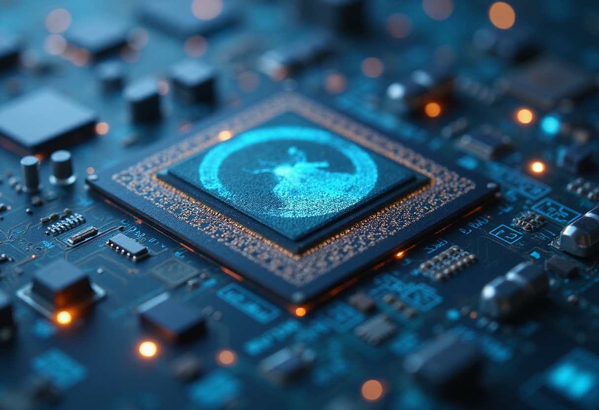
Intel plans to start mass production of its EMIB-T advanced packaging technology next year, according to a company roadmap that sets a target of assembling AI accelerators at up to 12 times reticle size. The figure is the headline claim of the roadmap: a single packaged device built from a dozen reticle-limited dies, stitched together rather than printed as one.
The target matters because reticle size, roughly 858 square millimeters on modern exposure tools, caps how large a monolithic die can be. Packaging several dies side by side is the only practical route beyond that ceiling. A 12x reticle package implies roughly 10,000 square millimeters of silicon per device, a scale at which only AI training accelerators justify the cost.
EMIB-T is Intel's bridge-die interconnect family with through-silicon vias added, allowing both horizontal die-to-die links and vertical stacking in one package. It sits alongside Foveros, Intel's 3D stacking technology, in a portfolio the company has pushed hard as a foundry differentiator. Rival foundries sell comparable services; TSMC's CoWoS and SoIC lines carry most of today's high-end AI silicon. Intel's argument is that it can offer the same class of integration on competitive terms.
What does the roadmap actually commit to?
The confirmed element is timing: EMIB-T reaches mass production next year. The 12x reticle figure is a target on a roadmap, not a shipping product, and the company has not named a customer for a package at that size. Readers should treat the two claims accordingly — one is a schedule, the other an ambition.
Intel's packaging roadmap has acquired commercial weight since the company began offering foundry customers access to its assembly lines. Advanced packaging capacity, not wafer capacity, has been the binding constraint on AI accelerator supply for the past two years, which is why a packaging schedule can move foundry negotiations as much as a process node announcement.
Why 12x reticle is the number to watch
Large language models reward larger accelerators. Nvidia's Blackwell generation already pairs two reticle-size dies in one package, and the industry consensus is that the next generation goes larger still. A 12x reticle package would roughly double the silicon area of the largest devices in volume production today.
The engineering risk sits in yield and warpage. Every additional die multiplies the chance that one bad component scraps the assembly, and large organic or silicon interposers bow under heat. EMIB-T's approach — small silicon bridges embedded in organic substrate, with TSVs where stacking is needed — is designed to reduce exactly that risk compared with a full-size silicon interposer.
Intel has not disclosed pricing, capacity figures, or named customers for EMIB-T volume production. The roadmap positions the technology against TSMC's expanding CoWoS family, where capacity remains allocated years ahead. If Intel delivers mass production on schedule, it becomes the second credible supplier at the high end of AI packaging. That alone changes the negotiating position of every accelerator designer currently queued at a single vendor.
The test arrives next year: whether EMIB-T ships in volume, and whether any customer commits to the 12x reticle extreme.
Source: Google News: AI chips
More from Nathan Brooks
Show full bio
Senior reporter covering people, launches and day-to-day practice in Semiconductors, chip manufacturing, hardware, AI compute at Chip Dispatch.
521 articles
Related articles
intel-malaysia-expands-advanced-packaging-as-ai-chips-grow-more-complex-137993ca
Intel Malaysia expands advanced packaging as AI chips grow more complex
asml-lines-up-intel-tsmc-and-samsung-behind-12-inch-masks-f70360a5
ASML Lines Up Intel, TSMC and Samsung Behind 12-Inch Masks
globalfoundries-to-manufacture-silicon-interposers-for-tsmc-355fc59d
GlobalFoundries to Manufacture Silicon Interposers for TSMC
globalfoundries-tsmc-align-on-us-silicon-interposers-for-ai-packaging-94aa0c50
GlobalFoundries, TSMC Align on US Silicon Interposers for AI Packaging