Gelsinger-Backed Nagare Labs Claims SRAM Speed at DRAM Density
Nagare Labs' capacitorless Z2RAM holds data 300 seconds at 85°C in founder papers, while Gen 1 claims of 5x SRAM density and 14x DRAM speed remain projections.
- By
- Rebecca Stone
- Filed
- Channel
- Memory & Storage
- Read
- 4 min read
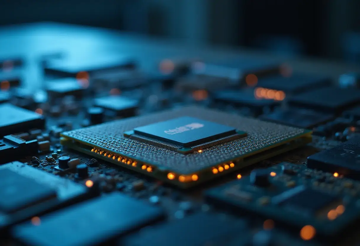
Nagare Labs, a Georgia Tech spinout with Pat Gelsinger on its board, is promising SRAM-speed memory at DRAM density, stacked directly on top of AI accelerators — and its founders' published papers show a cell that now retains data for more than 300 seconds at 85°C, up from 300 milliseconds five years ago. That measured leap is real. The headline numbers around it are not.
Gen 1 of the company's Z2RAM is projected, not measured, to deliver 5x SRAM density with six stacked layers, 14x DRAM speed, and 3x less read energy than SRAM. Nagare declined to share measured retention, latency, or energy figures for Z2RAM itself.
Why does anyone want memory on the compute?
AI chips are starved for bandwidth. HBM yields have been tight enough that some manufacturers reportedly plan fewer stacked layers just to ship product. Heat compounds the problem. Samsung's zHBM, which stacks DRAM straight onto the processor, is planned at only about four layers because of it.
Put DRAM on a logic die and the physics gets unforgiving: keeping the DRAM at or below 95°C caps the logic's heat output at 220 W/cm², or 300 W/cm² with better thermal vias, according to a 2025 simulation by co-founder Shimeng Yu's group at Georgia Tech. Micron's vHBM plans already include heat-spreading structures. Meanwhile, Nagare says peak compute has grown 70% a year for three decades against 20% for memory bandwidth.
What is Z2RAM, exactly?
"Two transistors and a shield. No capacitor," is how the company describes it. A write transistor puts charge on a storage node; the shield blocks noisy neighbors; the read transistor senses without draining. Reads are non-destructive, so the cell skips DRAM's write-back. Nagare targets well under a picojoule per bit.
The build is the interesting part. Layers get deposited on top of the accelerator and patterned "together on one die" — no interposer, no bonds between memory layers. One lithography exposure covers several layers, using standard 300 mm DUV tools. No EUV required. The roadmap points past 100 layers with "hundreds of thousands" of vertical connections.
What have the founders actually measured?
The paper trail shows fast progress. Suman Datta's group demonstrated a tungsten-doped indium oxide two-transistor cell at IEDM 2020 with retention of 1 second at 25°C — and just 300 ms at 85°C. A 2025 update added a third transistor and removed gate overlap, pushing retention past 1,000 seconds at 25°C, up from 200 seconds with overlapped devices. It also simulated a GPU L2 cache at twice SRAM's capacity in the same area, with a 75–80% lower energy-delay-area product.
Six months later, both founders showed a "folded asymmetric boosted" three-transistor cell holding data for over 300 seconds at 85°C, versus 100 milliseconds for a conventional design. The write pulse measured 10 ns. Simulated read delay was 2.6 ns in a 128×128 array at 7nm, with a projected cell area of 0.0168 µm² — against 0.0199 µm² for high-density SRAM on TSMC's N3. A separate Yu-group study found a four-tier, 256MB gain-cell cache at 7nm could hit 5.7x the bit density of 7nm SRAM in the same area. Returns fall off past seven or eight tiers as masks scale with layers; Nagare's single-lithography claim would sidestep that — if it works.
What could still go wrong?
Plenty. Nothing published demonstrates the single-exposure claim. Retention above 95°C — the DRAM thermal ceiling — remains unshown for every cell so far. "Where we are is literally lab prototypes," Datta told The Register. Tile sampling is targeted within four years; production shipments, if they arrive, within a decade. Yu said no standard exists yet for integrating this memory with an accelerator, so Nagare may have to define the interface itself. Single-electron effects can shift threshold voltages enough to upset stored bits. And the company has no fab — it's reportedly hunting for an R&D fab partner to scale beyond the university clean room, with AMD's 3D V-Cache cited as the working model for chipmaker collaboration.
The Gelsinger thread
Z2RAM follows Innovative Silicon's Z-RAM, which promised a similar 5x density gain 20 years ago, was licensed by AMD, and never pursued. Gelsinger, who phased out Intel's Optane in favor of CXL, now sits on Nagare's board. Playground Global, where he's a general partner, led the startup's $5 million round.
Until a fab-built, multi-layer stack is measured — 95°C retention included — Nagare's numbers stay on the roadmap, not on the wafer.
Source: Tom's Hardware
More from Rebecca Stone
Show full bio
Correspondent covering technology and product news in Semiconductors, chip manufacturing, hardware, AI compute at Chip Dispatch.
699 articles
Related articles
d-matrix-tapes-out-raptor-xpu-targets-10x-hbm4-bandwidth-364c686f
d-Matrix Tapes Out Raptor XPU, Targets 10x HBM4 Bandwidth
microsoft-s-new-ai-chip-nearly-triples-rack-level-hbm-report-says-9c2d6e51
Microsoft's New AI Chip Nearly Triples Rack-Level HBM, Report Says
samsung-and-sk-hynix-put-next-gen-ai-memory-on-show-at-chip-fair-82e646ea
Samsung and SK Hynix put next-gen AI memory on show at chip fair
ai-interposer-market-set-to-grow-40-fold-samsung-pushes-hbm4e-cooling-to-package-bfe8c8b4
AI Interposer Market Set to Grow 40-Fold; Samsung Pushes HBM4E Cooling to Package and System Level