Samsung's Lee Jae-yong Tours Yokohama Packaging Lab in AI Chip Push
Lee Jae-yong made his first visit to Samsung's Yokohama Advanced Package Lab, pressing researchers on packaging tech for AI chips, with ¥40 billion pledged.
- By
- Nathan Brooks
- Filed
- Channel
- Chip Manufacturing
- Read
- 2 min read
Samsung Electronics Executive Chairman Lee Jae-yong made his first visit on Nov. 1 to the company's Advanced Package Lab in Yokohama, roughly two months after the facility opened on Sept. 8. His message to researchers was direct: secure advanced packaging technologies, which he called a key to semiconductor competitiveness in the AI era.
The visit signals how Samsung intends to fight the AI chip war. The plan is to combine the company's semiconductor design and manufacturing strength with Japanese expertise in materials, components and equipment. Packaging, once an afterthought, now determines whether an AI system performs or merely functions.
Lee received a briefing from researchers on advanced packaging materials and process technologies, and discussed ways to work with Japan's semiconductor materials and equipment industry, Samsung said.
Why does packaging decide AI performance?
Advanced packaging integrates multiple semiconductors — GPUs, high-bandwidth memory (HBM) and accelerators — into a single package. How those chips connect affects data-processing bandwidth, power efficiency and thermal performance. A fast GPU paired with a slow package is a fast GPU throttled.
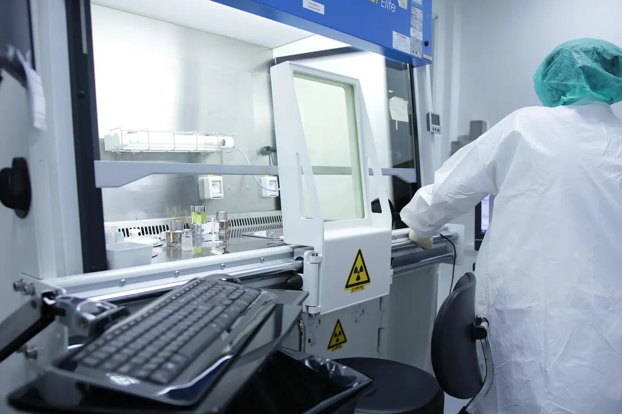
The Yokohama lab develops and validates the materials and process technologies this integration requires. It serves as a hub connecting Samsung's memory and logic technologies with those of Japanese materials, components and equipment firms.
Samsung established the lab, known as APL, in Yokohama in 2023. The company plans to invest ¥40 billion over five years starting in 2024, about 350 billion won, and to keep growing the local research staff.
What comes next in the research roadmap?
The scope of research will expand to next-generation processes and materials. On the agenda:
- Wafer-bonding technologies
- Glass substrates
- Potential research into new packaging structures for mass production of low-power, high-performance semiconductors
APL's remit differs from that of the packaging research organization inside Samsung's semiconductor research institute in South Korea. The two groups will work in separate areas while collaborating closely, on the theory that parallel efforts beat duplication.
Why Yokohama?
Samsung chose Japan for its packaging research base because the conditions for collaboration are unusually good. Japan hosts many companies with deep expertise in semiconductor materials, components and equipment, alongside an R&D base linked to universities and research institutions.
Yokohama itself has practical advantages. It sits close to Tokyo, which eases recruitment of specialized researchers, and hosts companies working on advanced packaging materials and equipment. Samsung intends to use the region's talent and its industry-academia-research network to turn APL into a hub for joint research with local firms.
Tokyo is doing its part. The Japanese government has designated semiconductors and AI as strategic industries and is pursuing investment and support policies. Samsung plans to build on that environment, expanding local collaboration and securing key materials and equipment technologies for advanced packaging.
The bet is straightforward. If packaging sets the ceiling on AI chip performance, Samsung has decided that the materials and tools to raise that ceiling are best found in Japan.
Source: Google News: AI chips
More from Nathan Brooks
Show full bio
Senior reporter covering people, launches and day-to-day practice in Semiconductors, chip manufacturing, hardware, AI compute at Chip Dispatch.
759 articles
Related articles
samsung-s-lee-jae-yong-tours-254-million-yokohama-packaging-lab
Samsung's Lee Jae-yong Tours $254 Million Yokohama Packaging Lab
samsung-foundry-bets-on-ai-chips-to-close-gap-with-tsmc-84321559
Samsung Foundry Bets on AI Chips to Close Gap With TSMC
samsung-weighs-chip-test-and-packaging-investment-in-vietnam-49f865a5
Samsung Weighs Chip Test and Packaging Investment in Vietnam
tsmc-intel-samsung-chase-ai-chip-barrier-via-early-integration-0bbd6a8e
TSMC, Intel, Samsung Chase AI Chip Barrier via Early Integration