Applied Materials Commits $5 Billion to EPIC Center in Silicon Valley
Applied Materials has unveiled a $5 billion EPIC Center in Silicon Valley, aiming to accelerate semiconductor innovation for the AI era. The figure is firm; the timeline is not yet.
- By
- Nathan Brooks
- Filed
- Channel
- Chip Manufacturing
- Read
- 3 min read
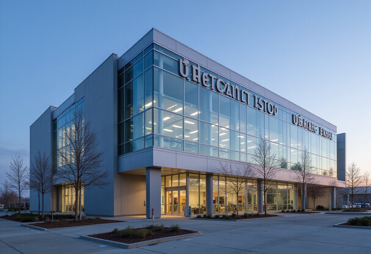
Applied Materials has unveiled plans for a $5 billion EPIC Center in Silicon Valley, a facility the company frames as its answer to the pace problem in AI-era chip development. The number is the headline. Five billion dollars buys a lot of concrete, and Applied intends to spend it on collaboration rather than volume production.
The announcement, reported by The Manila Times, positions the EPIC Center as a place where semiconductor innovation for the AI era can accelerate. That phrase carries weight in an industry where the distance between a research idea and a qualified manufacturing process is measured in years. Applied Materials supplies process equipment to nearly every major fab operator on earth, so its decision to fund a shared innovation campus tells us where it believes the bottleneck now sits: not in printing wafers, but in iterating on how they are printed.
What is the EPIC Center actually for?
The name stands for a coordinated research and prototyping environment, and the stated purpose is to bring equipment, materials and chip design decisions together under one roof. In practice, such facilities let customers and suppliers test process changes on real hardware before those changes reach a production line. The analogy is a wind tunnel for aircraft: cheap iteration on the ground, fewer surprises in the air.
For AI chips specifically, the commercial logic is direct. Training and inference hardware reward every improvement in transistor density, packaging and yield, and they punish delays. A shared center that shortens qualification cycles by even a few quarters can shift who wins a product generation.
Why Silicon Valley, and why now?
Locating the facility in Silicon Valley keeps it close to Applied's home base and to the system companies now designing their own silicon. The AI boom has pulled cloud providers and model builders directly into semiconductor roadmap decisions, and those customers want faster feedback loops than a conventional tool-vendor relationship provides.
The timing also reflects geography. With Washington pushing domestic semiconductor capacity through subsidies and export controls reshaping where advanced tools may ship, an onshore research campus is both a technical asset and a political one. Applied Materials, as a leading U.S. equipment maker, sits squarely in that current.
What remains unconfirmed
The announcement does not, on the evidence available, commit to specific capacity figures, wafer sizes or a firm operational date. The $5 billion figure is the hard number; the rest is intent. Readers should treat details about toolsets, staffing and partner participation as roadmap items until Applied publishes them.
The competitive read
Equipment makers rarely spend this kind of money on a single campus unless they expect it to lock in customer engagement. If the EPIC Center works as designed, Applied deepens its role at the earliest stage of process development, which tends to influence later tool purchasing. Rivals in deposition, lithography adjacency and metrology will notice.
The verdict, then, is straightforward. A five-billion-dollar bet on faster iteration is a bet that the AI era rewards speed over scale. Applied Materials has placed its chips; the industry will learn within a few years whether the center accelerates anything besides the company's own order book.
Source: Google News: semiconductors
More from Nathan Brooks
Show full bio
Senior reporter covering people, launches and day-to-day practice in Semiconductors, chip manufacturing, hardware, AI compute at Chip Dispatch.
368 articles
Related articles
applied-materials-puts-5-billion-into-silicon-valley-r-d-1545cc06
Applied Materials Puts $5 Billion Into Silicon Valley R&D
intel-and-tsmc-share-r-d-floor-at-applied-materials-epic-center-bad5eb1b
Intel and TSMC Share R&D Floor at Applied Materials EPIC Center
ucla-samueli-joins-applied-materials-epic-center-for-chip-r-d-f807cd4d
UCLA Samueli Joins Applied Materials' EPIC Center for Chip R&D
singapore-lands-7-8-billion-fab-with-44-000-wafers-a-month-output-0aa3deb2
Singapore Lands $7.8 Billion Fab With 44,000-Wafers-a-Month Output