UCLA Samueli Joins Applied Materials' EPIC Center for Chip R&D
UCLA Samueli will partner with Applied Materials' EPIC Center in Santa Clara, joining the equipment maker's academic network of process research targeting deposition, etch, and metrology work for advanced chip nodes.
- By
- Rebecca Stone
- Filed
- Channel
- Semiconductors
- Read
- 3 min read
UCLA Samueli School of Engineering will join Applied Materials' EPIC Center as a research partner, the organizations said, marking the latest academic collaboration at the equipment maker's flagship Silicon Valley research facility.
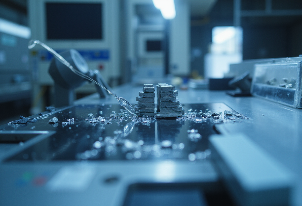
The EPIC Center — Equipment and Process Innovation and Commercialization — operates from Santa Clara, California. It houses production-scale deposition, etch, inspection, and metrology tools that Applied Materials makes available to chipmakers, materials suppliers, and academic researchers developing next-generation process technologies.
The center sits upstream of the company's commercial tool sales, which feed multi-billion-dollar fab build-outs at TSMC, Samsung, Intel, and the memory leaders SK hynix and Micron.
UCLA Samueli brings to the partnership a research portfolio covering semiconductor materials, device physics, photonics, and circuit design. Faculty at the school have published work spanning gate-all-around transistor architectures, neuromorphic computing substrates, and 3D heterogeneous integration.
The school also runs doctoral and master's programs that feed the semiconductor workforce in Southern California and across the broader U.S. chip industry.
What does the partnership change for Applied Materials?
Academic collaborations extend the equipment maker's visibility into early-stage process exploration. Universities working on sub-2 nm logic nodes — including backside power delivery, novel interconnect metals, and atomic-layer deposition recipes for high-NA EUV-compatible films — need access to deposition and etch systems that will define those devices.
Relationships of this kind typically translate into commercial process tools years after the academic research concludes. Applied Materials uses the academic channel to seed demand for the deposition, etch, and inspection systems it sells to high-volume manufacturing fabs, particularly as chipmakers prepare for the next round of node transitions and 3D DRAM scaling.
What does UCLA gain from access to EPIC?
Most university microfabrication facilities operate at older process nodes using donated or refurbished equipment. EPIC gives UCLA faculty and graduate students hands-on time with current-generation process tools alongside Applied Materials process engineers.
The arrangement also creates a recruiting pipeline. Applied Materials has historically hired process engineers and research scientists from its academic collaborators — a hiring channel that gains importance as competition for semiconductor talent intensifies under CHIPS Act workforce programs and as new fabs come online across Arizona, Ohio, and Texas.
How does this fit the broader chip R&D picture?
U.S. equipment makers have expanded academic partnerships since the CHIPS and Science Act of 2022 reshaped federal semiconductor research funding. The law authorized the National Semiconductor Technology Center, expanded advanced packaging programs, and increased DARPA and NSF research budgets — all of which favor industry-university consortia over single-institution projects.
EPIC collaborations sit alongside, rather than in competition with, the NSTC and similar public-private ventures. Applied Materials, Lam Research, Tokyo Electron, and ASML each maintain private R&D centers that compete for visibility with chipmakers' own internal development labs at Intel Foundry, TSMC, and Samsung.
What details remain undisclosed?
The announcement did not specify a financial commitment, the partnership's duration, or which UCLA research groups would lead initial projects. Applied Materials and UCLA have not published a joint technical roadmap or named principal investigators.
As logic nodes approach sub-2 nm and as chipmakers commit hundreds of billions of dollars to new fab capacity through the end of the decade, equipment vendors increasingly seed their future process pipelines through academic collaboration. Whether the UCLA-EPIC arrangement produces a specific process module or remains primarily a workforce and scouting effort will likely become clear within the first 18 to 24 months of joint projects.
Source: Google News: semiconductors
More from Rebecca Stone
Show full bio
Correspondent covering media and advertising at Chip Dispatch.
260 articles
Related articles
besi-joins-applied-materials-5-billion-epic-center-for-hybrid-bonding-7caa3559
Besi Joins Applied Materials' $5 Billion EPIC Center for Hybrid Bonding
arkansas-opens-research-institute-dedicated-to-semiconductor-innovation-c3c4d8e1
Arkansas Opens Research Institute Dedicated to Semiconductor Innovation
abm-opens-semiconductor-training-center-in-idaho-eda85a21
ABM Opens Semiconductor Training Center in Idaho
bangladesh-eyes-semiconductor-and-ai-partnership-with-arizona-state-university-fcf55a5a
Bangladesh Eyes Semiconductor and AI Partnership with Arizona State University