Applied Materials Bets $5 Billion on Next-Gen AI Chip Center
Applied Materials has opened a $5 billion R&D center to help chipmakers develop next-generation AI chips, one of the largest equipment-maker facility investments on record.
- By
- Rebecca Stone
- Filed
- Channel
- Chip Manufacturing
- Read
- 3 min read
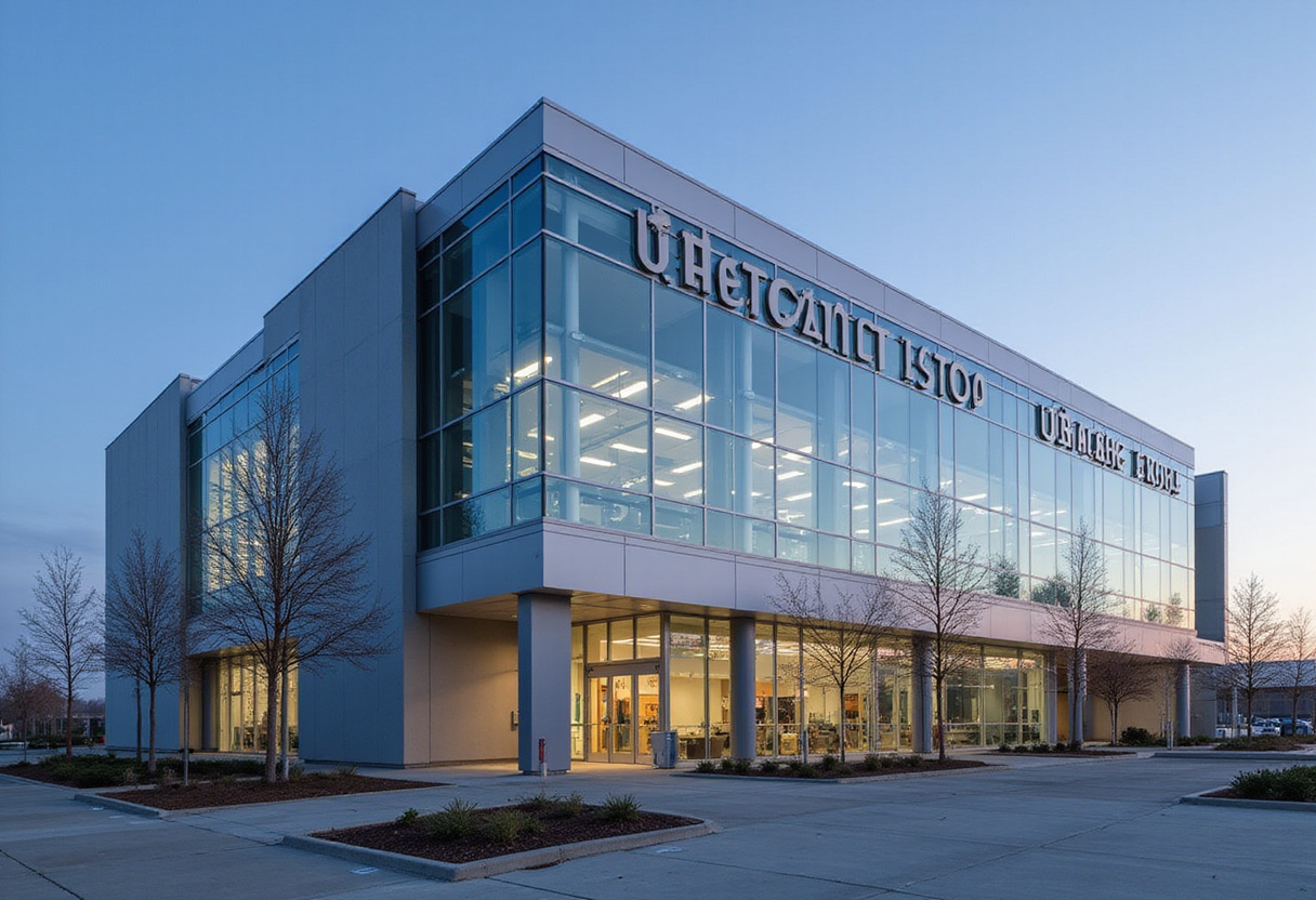
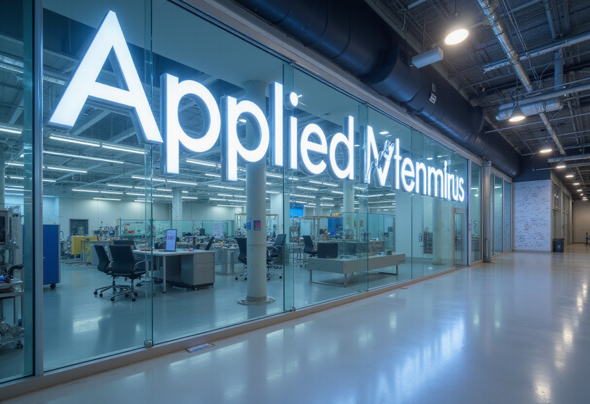
Applied Materials has opened a $5 billion research and development center aimed at helping its customers build the next generation of AI chips, the company announced. The figure, confirmed by the supplier itself, ranks among the largest single facility investments ever made by a semiconductor equipment maker.
That matters because of where Applied sits in the food chain. The company doesn't design chips. It builds the machines — deposition, etch, ion implant and metrology systems — that fabs such as TSMC, Samsung and Intel use to print circuits onto silicon. When AI accelerators push toward tighter geometries and new materials, the bottleneck often isn't the chip design. It's the process technology. Applied just spent $5 billion to attack exactly that bottleneck.
What is the center actually for?
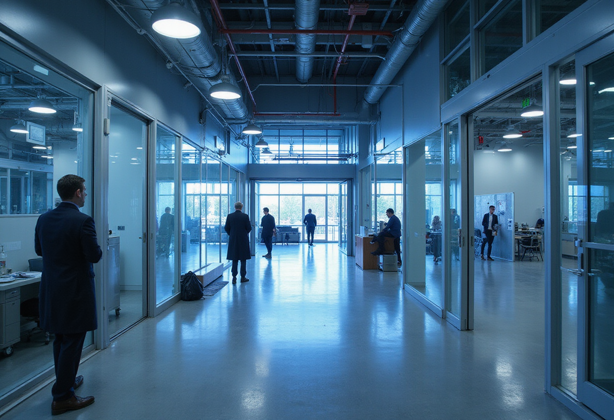
According to the company, the new facility will serve as a collaborative hub where chipmakers, materials suppliers and Applied's own engineers can work side by side on the process steps needed for future AI hardware. The idea is straightforward. Customers stop flying engineers between continents to debug a deposition recipe or a wafer-handling issue. Instead, they iterate on real wafers, on real tools, in one building.
That collaborative model shortens development cycles. It also gives Applied something arguably more valuable than the $5 billion price tag suggests: early visibility into what TSMC, Samsung and Intel will need two or three process generations out. Equipment makers live and die by roadmaps. A facility that puts customers' engineers on-site functions as a listening post for the entire industry's technical direction.
Why now?
The timing follows the money. AI chip demand has exploded over the past two years, with spending on accelerators and high-bandwidth memory straining capacity across the supply chain. Every leading-edge node now sold out. Every advanced packaging line booked. The constraints have shifted from lithography shine to the unglamorous layers beneath — materials engineering, interconnect, integration of chiplets and stacked dies.
Those are precisely Applied's strengths. The company's equipment portfolio covers the materials engineering steps that determine yield and performance at advanced nodes. As chipmakers stack logic and memory closer together to feed AI workloads, the number of deposition and etch steps per wafer keeps climbing. More steps per wafer means more tool sales per wafer. Applied's new center is, in part, a bet that this trend accelerates.
What does it change commercially?
For Applied's customers, the center promises faster qualification of new processes — fewer round trips between fab and vendor, quicker turns on experimental runs. For Applied's competitors, it raises the bar. Lam Research, Tokyo Electron and KLA all run their own customer-visit and demonstration programs, but few have committed capital at this scale to a single site.
The $5 billion commitment also signals confidence in the durability of AI-driven capex. Equipment makers don't spend that kind of money on a cyclical blip. They spend it when they believe a structural shift in demand has locked in a decade of tool purchases.
The road ahead
The center opens against a backdrop of record semiconductor investment worldwide, with governments in the U.S., Europe and Asia subsidizing new fabs and supply chains regionalizing under geopolitical pressure. Applied, headquartered in Santa Clara, California, now counts among the clearest beneficiaries of that build-out — and one of its most aggressive investors.
Whether the $5 billion hub pays off will show up gradually, in qualification cycles, co-development agreements and process-node transitions still on the drawing board. But the direction is clear: Applied is positioning itself not just as a tool vendor, but as the place where the next generation of AI silicon gets figured out.
If AI chip demand holds, the company will have bought itself a front-row seat — and a head start.
Source: Google News: AI chips
More from Rebecca Stone
Show full bio
Correspondent covering technology and product news in Semiconductors, chip manufacturing, hardware, AI compute at Chip Dispatch.
423 articles
Related articles
applied-materials-commits-5-billion-to-epic-center-in-silicon-valley-606a1ebf
Applied Materials Commits $5 Billion to EPIC Center in Silicon Valley
applied-materials-commits-5-billion-to-silicon-valley-r-d-hub-322e5cec
Applied Materials Commits $5 Billion to Silicon Valley R&D Hub
applied-materials-commits-5-billion-to-silicon-valley-ai-chip-research-hub-0d3e3c8a
Applied Materials Commits $5 Billion to Silicon Valley AI Chip Research Hub
applied-materials-puts-5-billion-into-silicon-valley-r-d-centre-aae52578
Applied Materials Puts $5 Billion Into Silicon Valley R&D Centre