Applied Materials Puts $5 Billion Into Silicon Valley R&D Centre
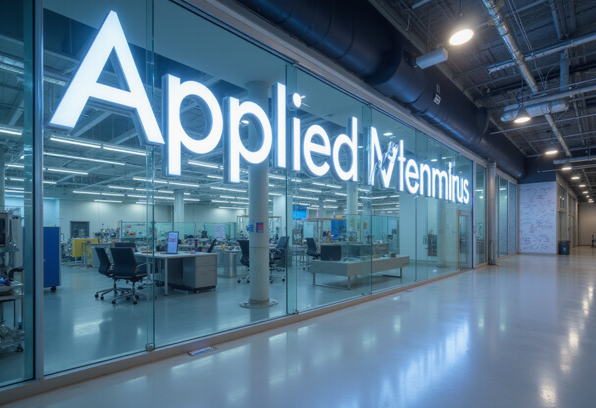
Applied Materials has opened a $5 billion semiconductor R&D centre in Silicon Valley, its largest single US research commitment, aimed at shortening the road from materials science to fab-ready tools.
- By
- Nathan Brooks
- Filed
- Channel
- Chip Manufacturing
- Read
- 2 min read
Applied Materials has opened a $5 billion semiconductor research and development centre in Silicon Valley. The figure is the largest single R&D commitment the equipment maker has announced at one US site, and it lands in a year when Washington is spending heavily to pull advanced chipmaking back onto American soil.
The company announced the opening through a report carried by Electronics For You. The centre gives Applied Materials a dedicated space to develop next-generation process equipment and materials alongside chipmakers, materials suppliers and researchers. That model matters. Equipment development has become a joint exercise, because transistor and packaging advances now depend on tools, chemistries and integration schemes evolving together rather than in sequence.
What does a $5 billion lab actually buy?
The short answer is time. Process equipment is the bottleneck through which every new node must pass. When a tool vendor can test materials and integration steps in-house, before customers commit wafer capacity, the whole development cycle shortens. A central R&D site lets Applied Materials run those experiments at scale, under one roof, with its customers' engineers in the room.
The location is not incidental. Silicon Valley remains the densest cluster of semiconductor design and materials talent in the United States, even after decades of manufacturing moving to East Asia. Building the centre there keeps the company close to the universities, startups and device makers that shape its roadmap.
Why now?
The timing follows the US government's push to rebuild domestic semiconductor capability, which has redirected billions in subsidies toward fabs and, less visibly, toward the supply base that equips them. Applied Materials sits squarely in that supply base. Its deposition, etch and inspection tools ship into nearly every advanced logic and memory fab in the world, so any broadening of US capacity tends to broaden its addressable market.
There is also a competitive reading. Rivals ASML, Lam Research and Tokyo Electron continue to pour money into their own research operations, and the race to define equipment for gate-all-around transistors, backside power delivery and advanced packaging is already under way. A $5 billion facility signals that Applied Materials intends to set that agenda rather than follow it.
The verdict
The centre is a research investment, not a production plant. No wafer capacity, revenue figure or hiring target accompanied the announcement, so any economic impact remains a projection rather than a fact. Still, the scale of the commitment is unambiguous. In an industry where the tool maker's roadmap quietly dictates what the chipmaker can build, Applied Materials has just bought itself a considerably larger drafting table.
Source: Google News: semiconductors
More from Nathan Brooks
Show full bio
Senior reporter covering people, launches and day-to-day practice in Semiconductors, chip manufacturing, hardware, AI compute at Chip Dispatch.
432 articles
Related articles
applied-materials-commits-5-billion-to-silicon-valley-ai-chip-research-hub-0d3e3c8a
Applied Materials Commits $5 Billion to Silicon Valley AI Chip Research Hub
applied-materials-commits-5-billion-to-silicon-valley-r-d-hub-322e5cec
Applied Materials Commits $5 Billion to Silicon Valley R&D Hub
applied-materials-puts-5-billion-into-silicon-valley-r-d-1545cc06
Applied Materials Puts $5 Billion Into Silicon Valley R&D
applied-materials-bets-5-billion-on-next-gen-ai-chip-center-7af279be
Applied Materials Bets $5 Billion on Next-Gen AI Chip Center