Applied Materials Puts $5 Billion Into Silicon Valley R&D
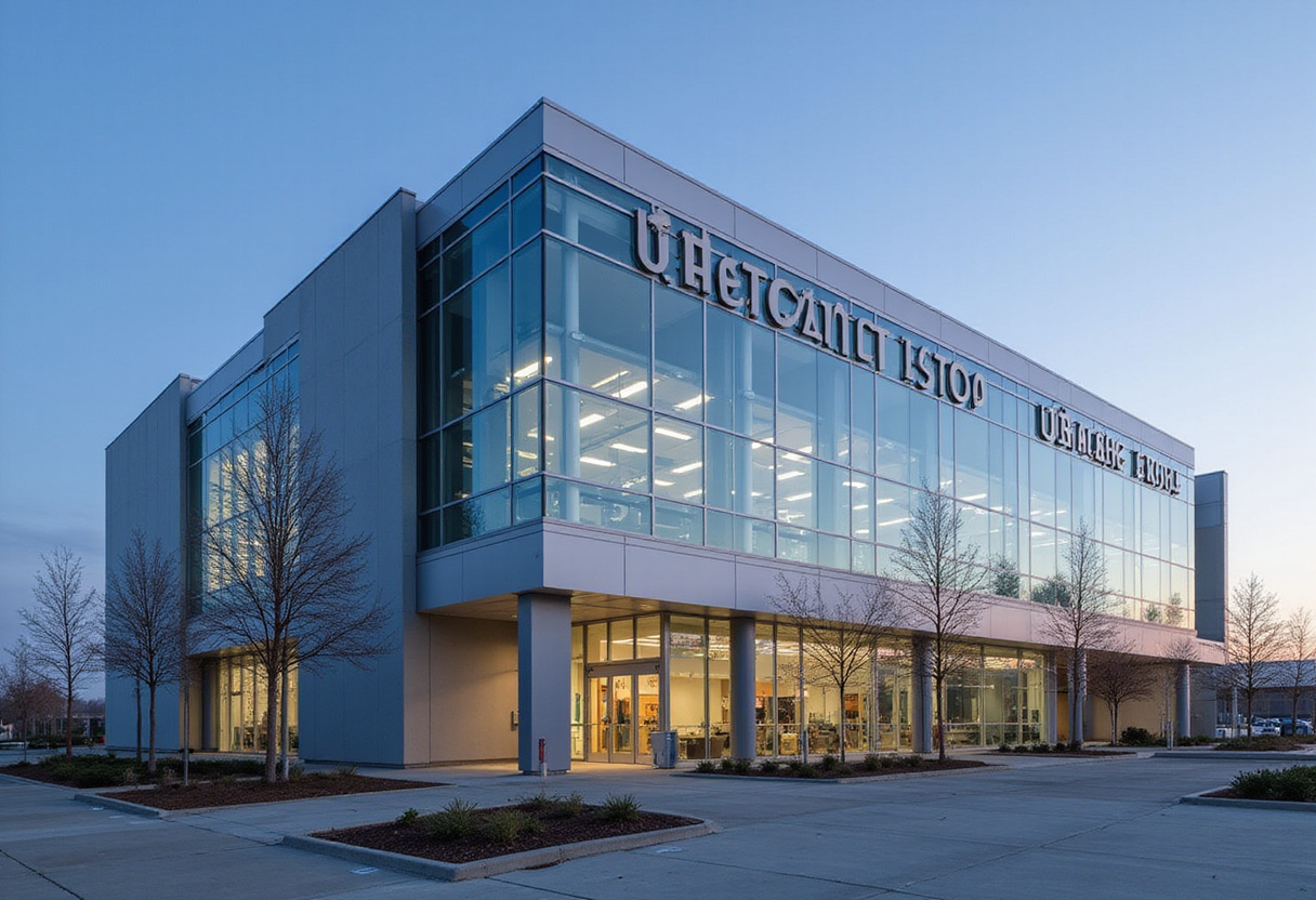
Applied Materials has opened a $5 billion semiconductor research and development center, betting that process tool innovation, not just chip design, will decide the next decade of silicon.
- By
- Nathan Brooks
- Filed
- Channel
- Chip Manufacturing
- Read
- 3 min read
Applied Materials has opened a $5 billion semiconductor research and development center, the company announced. That figure makes the facility one of the largest private R&D commitments in the chip equipment industry, and it lands at a moment when toolmakers, not chip designers, hold the narrowest bottleneck in the supply chain.
The announcement itself is brief. The $5 billion number is the concrete fact on the table; the company has not, in this release, broken the figure down into construction cost, tool installations, or staffing. Treat the sum as a total program commitment until Applied Materials publishes further detail. What is confirmed is the purpose: a dedicated center for semiconductor research and development, operated by the largest equipment supplier in the industry.
Why would a toolmaker spend this much on R&D?
The economics of the equipment business explain the move. Every advance in logic and memory now depends on new deposition, etch, and metrology steps at each process node. Chipmakers approaching two-nanometer-class production cannot buy progress off the shelf. They need tools co-developed years in advance, and the toolmaker that co-develops them first tends to win the order book that follows.
A centralized R&D center also gives customers a place to qualify processes before committing wafer volume. For fabs, that de-risks new nodes. For Applied Materials, it embeds the company earlier in each customer's roadmap than a standard vendor relationship allows. The strategy is straightforward: own the development phase, and the purchase orders follow.
What does it signal about the market?
A $5 billion bet is a statement about demand durability. Equipment makers do not commit capital of this size for a cyclical blip. The decision implies Applied Materials expects sustained investment in leading-edge logic and advanced memory across multiple years, spanning fabs in the United States, Asia, and the new capacity being built in Europe and Japan.
There is a geopolitical reading as well. Governments in Washington, Brussels, and Tokyo are subsidizing fab construction, and every new fab needs a tool line. An R&D base of this scale positions the company to serve, and to be seen serving, regional capacity programs rather than watching from the sidelines. The commercial picture and the policy picture point the same direction here.
The competitive angle
Applied Materials competes chiefly with ASML, Lam Research, and Tokyo Electron across deposition, etch, and related process steps. Each of those rivals funds substantial research of its own, and none of them treats R&D as optional. What distinguishes this announcement is the size and the single-site concentration of the commitment. Rivals may answer with equivalent investments; they have not announced one at this figure today.
Investors should note the distinction between a capital commitment and revenue. The $5 billion builds capability over years. It converts to sales only as customers adopt the processes the center helps qualify. That lag is normal for the industry, and it cuts both ways: slow qualification delays payback, fast adoption compresses it.
The verdict, then: a large company has spent a large sum on the least glamorous and most defensible layer of the semiconductor stack. Whether the $5 billion center becomes the industry's shared workshop or an expensive showroom will depend on how quickly customers bring their next nodes through its doors — and on that, the roadmap, not the ribbon-cutting, will pass judgment.
Nathan Brooks is a senior editor at Chip Dispatch.
Source: Google News: semiconductors
More from Nathan Brooks
Show full bio
Senior reporter covering people, launches and day-to-day practice in Semiconductors, chip manufacturing, hardware, AI compute at Chip Dispatch.
368 articles
Related articles
applied-materials-commits-5-billion-to-epic-center-in-silicon-valley-606a1ebf
Applied Materials Commits $5 Billion to EPIC Center in Silicon Valley
intel-and-tsmc-share-r-d-floor-at-applied-materials-epic-center-bad5eb1b
Intel and TSMC Share R&D Floor at Applied Materials EPIC Center
sia-maps-supply-chain-gaps-threatening-u-s-chip-ecosystem-061afb10
SIA Maps Supply Chain Gaps Threatening U.S. Chip Ecosystem
tsmc-prepares-to-pour-265-billion-into-u-s-fab-buildout-762fb55c
TSMC Prepares to Pour $265 Billion Into U.S. Fab Buildout