Applied Materials Commits $5 Billion to Silicon Valley AI Chip Research Hub
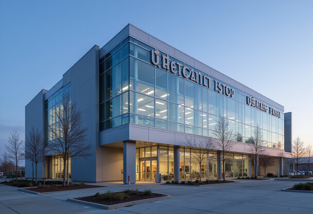
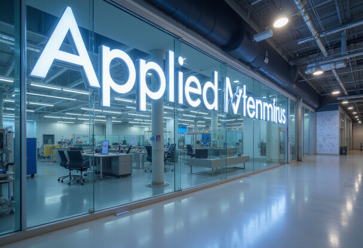
Applied Materials has unveiled a $5 billion research facility in Silicon Valley, aiming to streamline AI chipmaking through collaborative development of tools, materials and processes.
- By
- Grace Kim
- Filed
- Channel
- Chip Manufacturing
- Read
- 2 min read
Applied Materials has unveiled a $5 billion research facility in Silicon Valley. The company says the investment aims to streamline how AI chips are made.
The announcement puts a hard number on one of the larger research commitments in the U.S. toolmaking sector. Applied Materials builds the deposition, etch and inspection equipment that fabs depend on. Its customers include the leading logic and memory manufacturers now racing to add AI-related capacity.
What does the facility do?
The company frames the site as a collaborative research center. The goal is to bring chip designers, equipment engineers and material suppliers onto one campus. That proximity, Applied Materials argues, shortens the loop between process development and volume production.
The initiative targets the specific bottlenecks of AI chipmaking. Advanced AI processors stack more layers, use new materials and push process integration harder than prior generations. Each of those steps depends on tool and material co-optimization.
Why locate it in Silicon Valley?
Applied Materials is headquartered in Santa Clara, California. Placing the $5 billion facility in Silicon Valley keeps the research effort adjacent to the company's core engineering base. It also sits near many of the architects of the current AI boom.
The region remains the design center of the global semiconductor industry, even as most advanced manufacturing sits in Taiwan, South Korea and — increasingly — Arizona. A research site in California addresses development, not wafer output.
How does it fit the AI supply picture?
Demand for AI accelerators has strained every segment of the supply chain, from advanced packaging to high-bandwidth memory to leading-edge logic capacity. Equipment makers sit upstream of all of it. Faster process development at the tool stage can translate into faster yield ramps at the fab stage.
Applied Materials does not state a target production node or a capacity figure for the facility. The $5 billion figure refers to the research investment itself. This is a development play, not a manufacturing expansion.
What remains unclear?
The company has not detailed a construction timeline, staffing level or specific tool platforms slated for the site. Until it does, the $5 billion commitment stands as a directional signal rather than a dated roadmap.
Analysts have long argued that AI-era chip complexity demands closer collaboration across the supply chain. Applied Materials is now backing that view with its own capital. The facility's success will be measured by whether it compresses the time from process concept to qualified production for the next generation of AI silicon.
Source: Google News: TSMC
More from Grace Kim
Show full bio
Market editor covering people, launches and day-to-day practice in Semiconductors, chip manufacturing, hardware, AI compute at Chip Dispatch.
401 articles
Related articles
applied-materials-commits-5-billion-to-silicon-valley-r-d-hub-322e5cec
Applied Materials Commits $5 Billion to Silicon Valley R&D Hub
applied-materials-commits-5-billion-to-epic-center-in-silicon-valley-606a1ebf
Applied Materials Commits $5 Billion to EPIC Center in Silicon Valley
ucla-samueli-joins-applied-materials-epic-center-for-chip-r-d-f807cd4d
UCLA Samueli Joins Applied Materials' EPIC Center for Chip R&D
intel-and-tsmc-share-r-d-floor-at-applied-materials-epic-center-bad5eb1b
Intel and TSMC Share R&D Floor at Applied Materials EPIC Center