Applied Materials Opens $5 Billion Semiconductor Innovation Center
Applied Materials has opened a $5 billion semiconductor innovation center, one of the largest equipment-maker R&D commitments on record.
- By
- Grace Kim
- Filed
- Channel
- Chip Manufacturing
- Read
- 3 min read
Applied Materials has opened a $5 billion semiconductor innovation center. The company confirmed the facility's completion this week. The sum ranks among the largest single commitments an equipment maker has placed in chip research infrastructure.
The center consolidates process development work under one roof. Applied Materials supplies deposition, etch, implant and metrology tools to nearly every major fab operator. Its customers include leading-edge logic and memory producers worldwide.
Why does a $5 billion R&D site matter?
Equipment development and chipmaker roadmaps have grown inseparable. New transistor architectures demand new tool chemistries before volume production can begin. Co-locating engineers from toolmaker and customer shortens that loop.
The investment lands during a broad buildout of fab capacity across the United States, Asia and Europe. Governments are subsidizing new plants. Equipment vendors decide, in practice, how fast those plants ramp. Applied Materials holds one of the three largest shares of the wafer-fab-equipment market alongside ASML and Lam Research.
What can the center do?
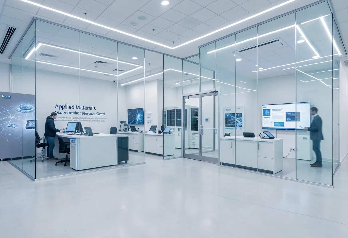
The company describes the site as a hub for collaborative innovation. Customers and suppliers can work alongside Applied engineers on next-generation process modules. That model mirrors the joint development programs that major chipmakers already run with their capital-equipment partners.
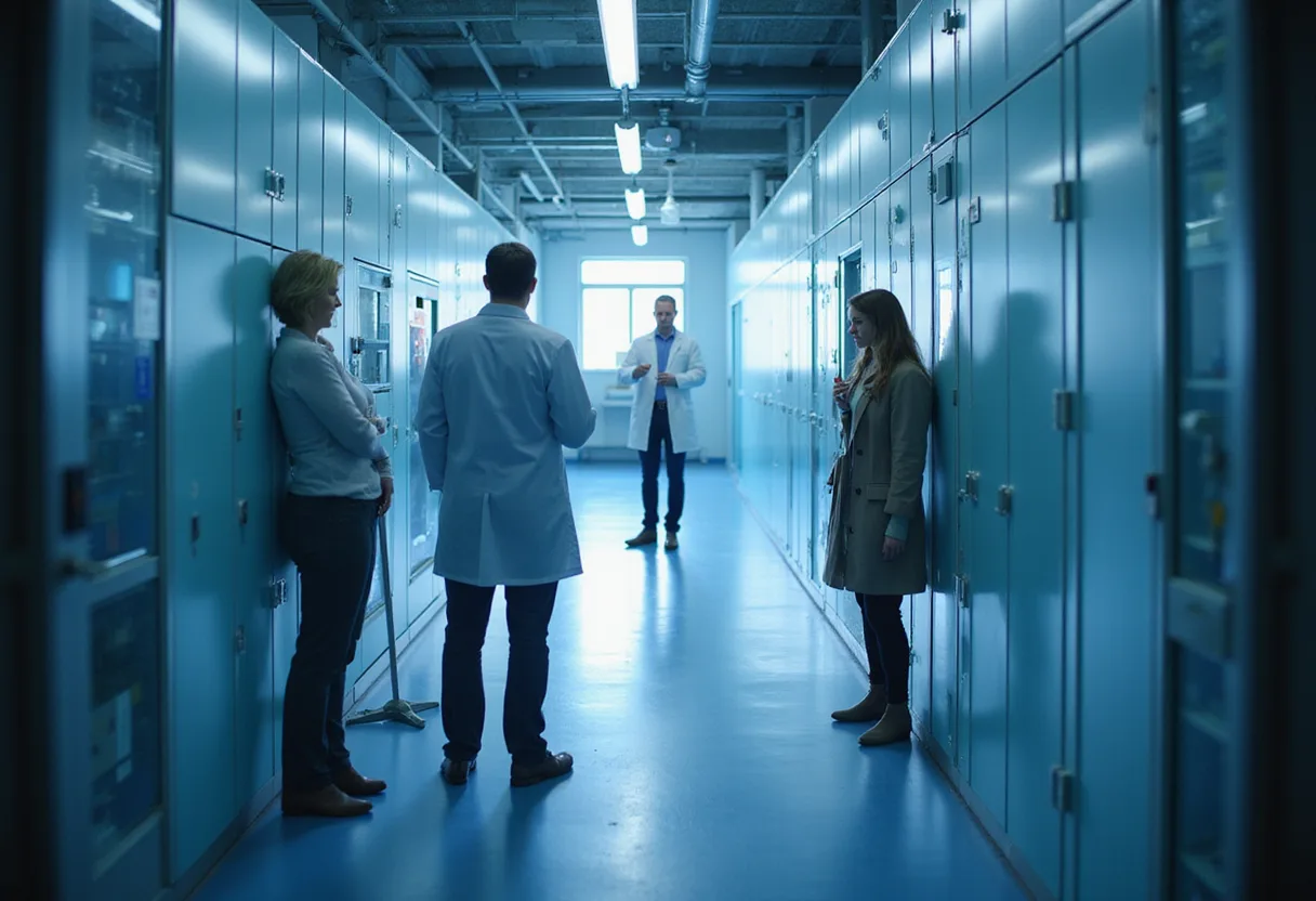
A facility of this scale typically houses cleanroom space, pilot toolsets and laboratories. Applied Materials has not itemized the square footage or tool count in the announcement. It has positioned the $5 billion figure as the headline commitment.
How does this fit the competitive picture?
Applied Materials earns the majority of its revenue from systems that build and inspect chip layers. Demand tracks wafer starts at its customers' fabs. Any tool that speeds the path from design to high-volume manufacturing adds pricing power.
Rival equipment makers have made comparable bets on expanded R&D footprints. The industry's revenue has cycled upward on spending for artificial-intelligence processors, advanced packaging and memory. A dedicated innovation center gives Applied a standing venue to demonstrate new tools before purchase orders exist.
Geopolitics shapes the backdrop. Export controls restrict which Chinese customers may buy which American tools. That constraint pushes vendors to extract more value from permitted markets and from collaborative development with allied-region fabs. A domestic innovation center supports that strategy.
What comes next?
The center opens as equipment spending forecasts diverge by segment. Logic and packaging investment remains firm. Memory orders fluctuate with pricing cycles. Applied Materials has tied the facility to long-term process innovation rather than any single product family.
The company has framed the site as a place where the industry can prototype tomorrow's manufacturing steps at scale. Success will show up in tool qualification timelines and in the depth of customer programs it hosts. Watch for the first named development partners and pilot projects as early signals of the center's pull.
By Grace Kim, Chip Dispatch.
Note: This report is based on the announcement headline. Manufacturing Dive's full article contains additional detail on the facility's scope and timing.
Source: Google News: semiconductors
More from Grace Kim
Show full bio
Market editor covering people, launches and day-to-day practice in Semiconductors, chip manufacturing, hardware, AI compute at Chip Dispatch.
544 articles
Related articles
applied-materials-puts-5-billion-into-silicon-valley-r-d-center-16883488
Applied Materials Puts $5 Billion Into Silicon Valley R&D Center
applied-materials-puts-5-billion-into-silicon-valley-r-d-1545cc06
Applied Materials Puts $5 Billion Into Silicon Valley R&D
applied-materials-puts-5-billion-behind-shared-chip-research-659b6fc6
Applied Materials Puts $5 Billion Behind Shared Chip Research
applied-materials-commits-5-billion-to-silicon-valley-r-d-hub-322e5cec
Applied Materials Commits $5 Billion to Silicon Valley R&D Hub