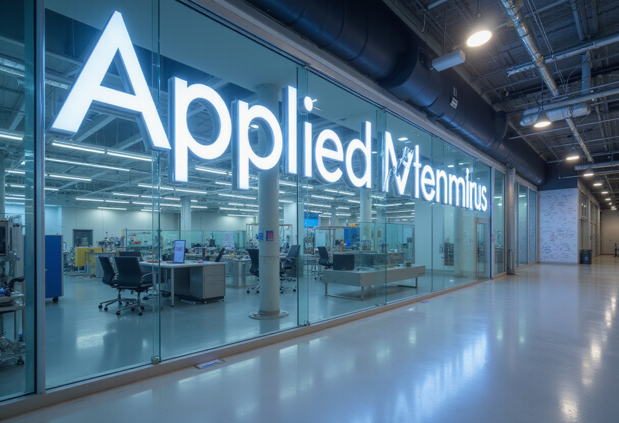
Applied Materials Puts $5 Billion Behind Shared Chip Research
Applied Materials has opened a new $5 billion research facility built around collaborative semiconductor innovation, aiming to shorten the loop between lab results and production tools.
- By
- Nathan Brooks
- Filed
- Channel
- Chip Manufacturing
- Read
- 2 min read
Applied Materials has opened a new $5 billion chip research facility, betting that the next generation of semiconductors will be developed jointly rather than in isolation. The sum is the hardest number in the story, and it is a confirmed investment, not a roadmap item. For context, five billion dollars buys roughly a mid-sized fab's worth of tooling; here it buys a building where equipment makers, chipmakers and researchers are meant to work in the same rooms.
The company framed the facility as a way to accelerate collaborative semiconductor innovation. That phrasing carries real weight in an industry where the distance between a process idea and a production-worthy tool is measured in years. Shared research space shortens that distance by putting the people who build deposition and etch systems next to the people who must integrate them into advanced nodes.
Why does collaborative research matter to equipment makers?
Applied Materials does not sell chips. It sells the machines that make chips, and its fortunes track the process roadmaps of its customers. When transistor structures, materials and stacking schemes grow more exotic, the tools must change alongside them. A joint research site lets Applied Materials and its partners debug that interplay early.
The commercial logic is straightforward. If a new material combination works in the shared lab, the tool that enabled it arrives first from Applied Materials. Equipment vendors compete on exactly that kind of head start, and a $5 billion facility is a durable way to buy one.
What does the timing tell us?
The opening lands amid heavy global spending on chip capacity, with governments in the United States, Europe and Asia subsidizing fabs and research alike. Equipment suppliers sit upstream of all of it. Every new fab announcement, wherever it is built, eventually becomes an order for deposition, etch and inspection tools.
A research facility is a quieter commitment than a fab, but it is a longer one. Fabs serve a demand cycle; research infrastructure serves a decade. Applied Materials is signaling that it expects the industry's materials and integration problems to keep getting harder, and that it intends to be paid to help solve them.
The company's own description emphasizes acceleration. In practice, that means shortening the loop between an experimental result and an engineering decision. Whether the facility produces publishable breakthroughs or quietly improved tool attachments, the value accrues to whoever holds the keys.
What comes next?
Expect the facility's worth to show up not in headlines but in process-cycle times at its partners' fabs. If collaboration works as advertised, advanced-node customers will qualify new steps faster, and Applied Materials will defend its position at the top of the equipment market it already leads.
Source: Google News: semiconductors
More from Nathan Brooks
Show full bio
Senior reporter covering people, launches and day-to-day practice in Semiconductors, chip manufacturing, hardware, AI compute at Chip Dispatch.
414 articles
Related articles
applied-materials-puts-5-billion-into-silicon-valley-r-d-1545cc06
Applied Materials Puts $5 Billion Into Silicon Valley R&D
applied-materials-commits-5-billion-to-epic-center-in-silicon-valley-606a1ebf
Applied Materials Commits $5 Billion to EPIC Center in Silicon Valley
singapore-targets-the-lab-to-fab-gap-in-semiconductors-813f892d
Singapore Targets the Lab-to-Fab Gap in Semiconductors
applied-materials-commits-5-billion-to-silicon-valley-ai-chip-research-hub-0d3e3c8a
Applied Materials Commits $5 Billion to Silicon Valley AI Chip Research Hub