Engineering the World's Largest AI Chips: From Blueprint to Build
Semiconductor Engineering's feature traces how reticle-busting, multi-die AI accelerators move from first architecture sketch to packaged, deployed silicon.
- By
- Rebecca Stone
- Filed
- Channel
- AI & Compute
- Read
- 2 min read
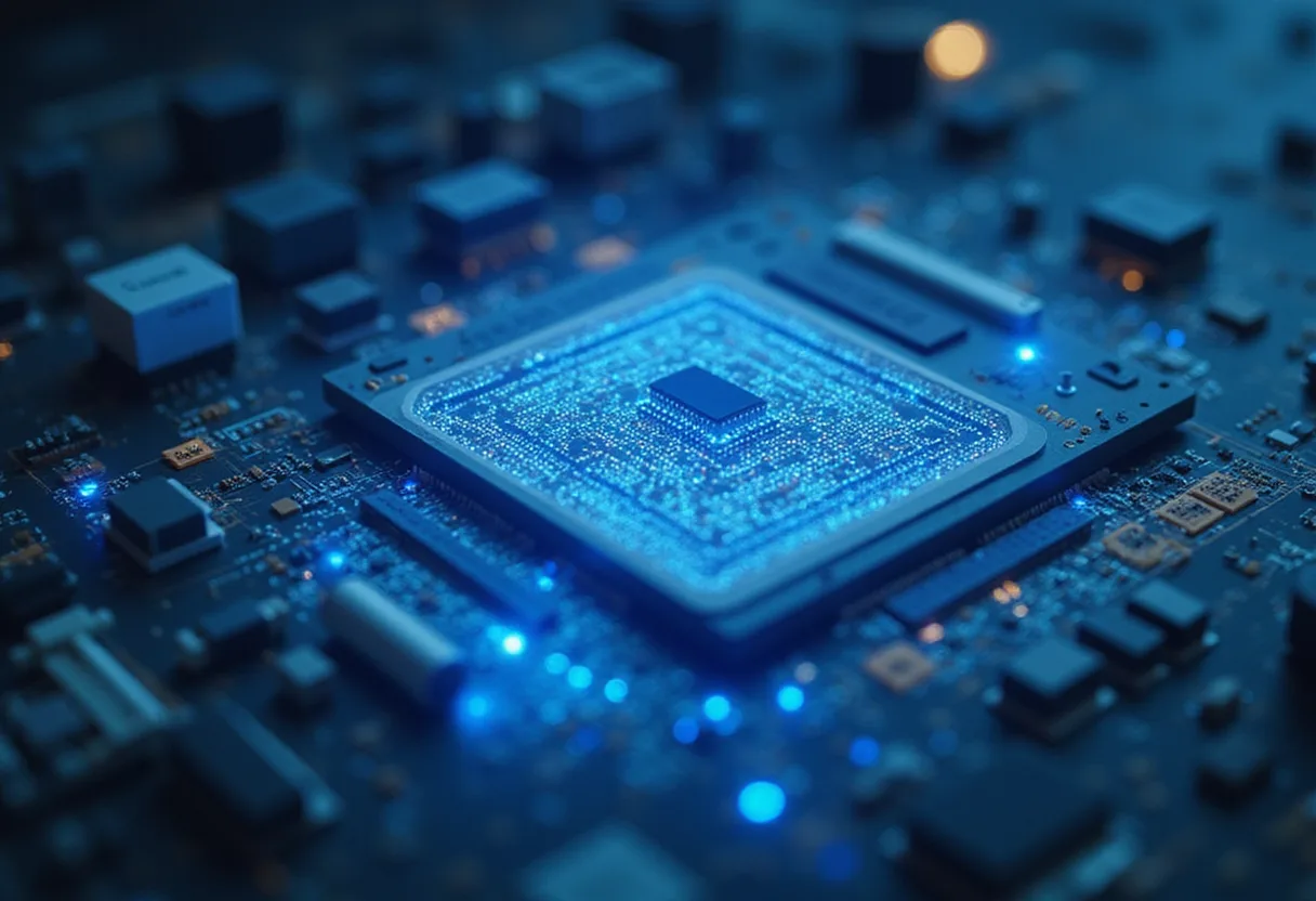
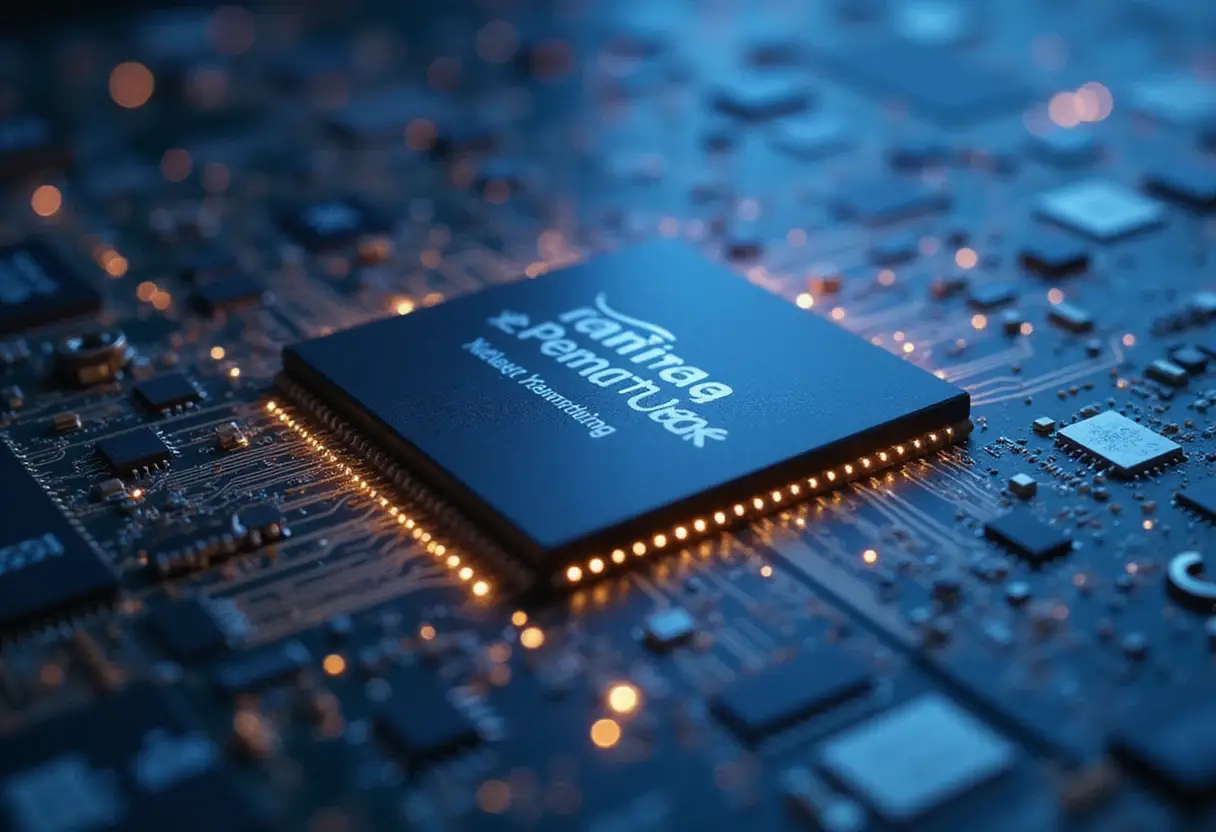
The world's largest AI chips now stretch reticle limits, span multiple dies on a single package, and demand packaging, test and cooling decisions that start on day one of the design cycle. That is the subject of Semiconductor Engineering's feature "From Blueprint To Build: Engineering The World's Largest AI Chips," which walks through how these massive devices move from architecture sketches to shipping silicon.
Why does chip size change everything? Because a giant AI accelerator is no longer a single piece of silicon in any practical sense. The article frames the central shift: as AI chips grew beyond what one die can hold, engineering teams had to reorganize the entire build process around multi-die designs, advanced packaging and the supply chain that holds it all together.
What does the build actually involve?
The feature traces the journey in stages, and each stage compounds the last:
- Architecture and planning, where die counts, memory placement and interconnect strategy get locked in early.
- Design and verification, where a chip the size of a small wafer section strains tooling, simulation times and engineering schedules.
- Manufacturing and packaging, where multi-die assemblies push substrates, interposers and bonding processes to their limits.
- Test, qualification and deployment, where thermal and power constraints in the datacenter feed back into decisions made months earlier at the blueprint stage.
Why now?
The piece situates this engineering story inside the AI boom. Training and inference clusters keep demanding more compute per package, and the industry's answer has been to make each package bigger — more dies, more memory stacked closer to the logic, more power flowing through a single lidded rectangle. That growth, the article makes clear, is not just a marketing race. It rewrites how foundries, OSATs, EDA vendors and chip architects divide the work.
The through-line of the feature is coordination. A chip this large fails not because any one step is impossible, but because the steps stop talking to each other. Packaging choices constrain thermal design. Thermal design constrains datacenter deployment. Datacenter constraints loop back into the next chip's blueprint. The article's argument is that the biggest AI silicon of this generation is engineered as a system problem from the first whiteboard sketch, not assembled from parts at the end.
Who should read it?
Semiconductor Engineering pitches the piece at practitioners: architects wrestling with partitioning, packaging engineers watching substrate technology advance under them, and supply-chain planners mapping capacity for dies, interposers and high-bandwidth memory. It reads as a status report on where the toolchain and the manufacturing base currently stand, rather than a roadmap with promised ship dates.
The article closes its arc where the industry now lives: with each generation of AI silicon, the boundary between "chip" and "system" keeps dissolving, and the companies that master the blueprint-to-build pipeline — not just the architecture — will decide who can actually deliver the largest AI chips at scale.
Source: Google News: AI chips
More from Rebecca Stone
Show full bio
Correspondent covering technology and product news in Semiconductors, chip manufacturing, hardware, AI compute at Chip Dispatch.
669 articles
Related articles
digitimes-ai-scaling-shifts-from-die-shrinks-to-system-integration-2af5109e
DIGITIMES: AI Scaling Shifts From Die Shrinks to System Integration
intel-targets-12x-reticle-size-ai-chips-as-emib-t-enters-mass-production-acc00c7d
Intel Targets 12x Reticle-Size AI Chips as EMIB-T Enters Mass Production
applied-materials-bets-on-ai-demand-to-drive-equipment-sales-through-2030-b3e71079
Applied Materials Bets on AI Demand to Drive Equipment Sales Through 2030
tsmc-intel-samsung-chase-ai-chip-barrier-via-early-integration-0bbd6a8e
TSMC, Intel, Samsung Chase AI Chip Barrier via Early Integration