GlobalFoundries to Operate Two New US Fabs Under US-Japan Pact
GlobalFoundries will operate two new US fabs under a US-Japan government pact, extending its domestic specialty foundry footprint under bilateral backing.
- By
- Grace Kim
- Filed
- Channel
- Chip Manufacturing
- Read
- 2 min read
GlobalFoundries will operate two new fabs in the United States under a pact between the US and Japanese governments. The arrangement names the foundry as operator for both facilities. It marks a concrete step in the two countries' cooperation on semiconductor manufacturing.
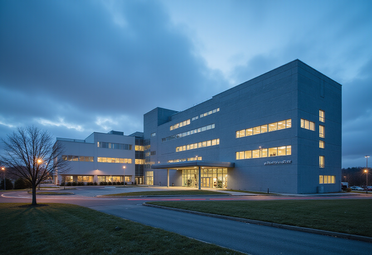
The deal places GlobalFoundries, the world's largest pure-play specialty foundry by some measures and a major US-based contract chipmaker, at the center of a government-backed capacity expansion. Both new fabs will sit on American soil. The company already runs US manufacturing, including its Malta, New York, campus, so the new sites extend an established domestic footprint rather than starting one.
What does the pact signal?
Governments have rarely named a specific commercial operator inside a bilateral semiconductor agreement. Doing so here moves the US-Japan pact from policy language toward committed production capacity. For customers, that distinction matters: a designated operator means a defined process portfolio, wafer supply agreements and qualification timelines can begin.
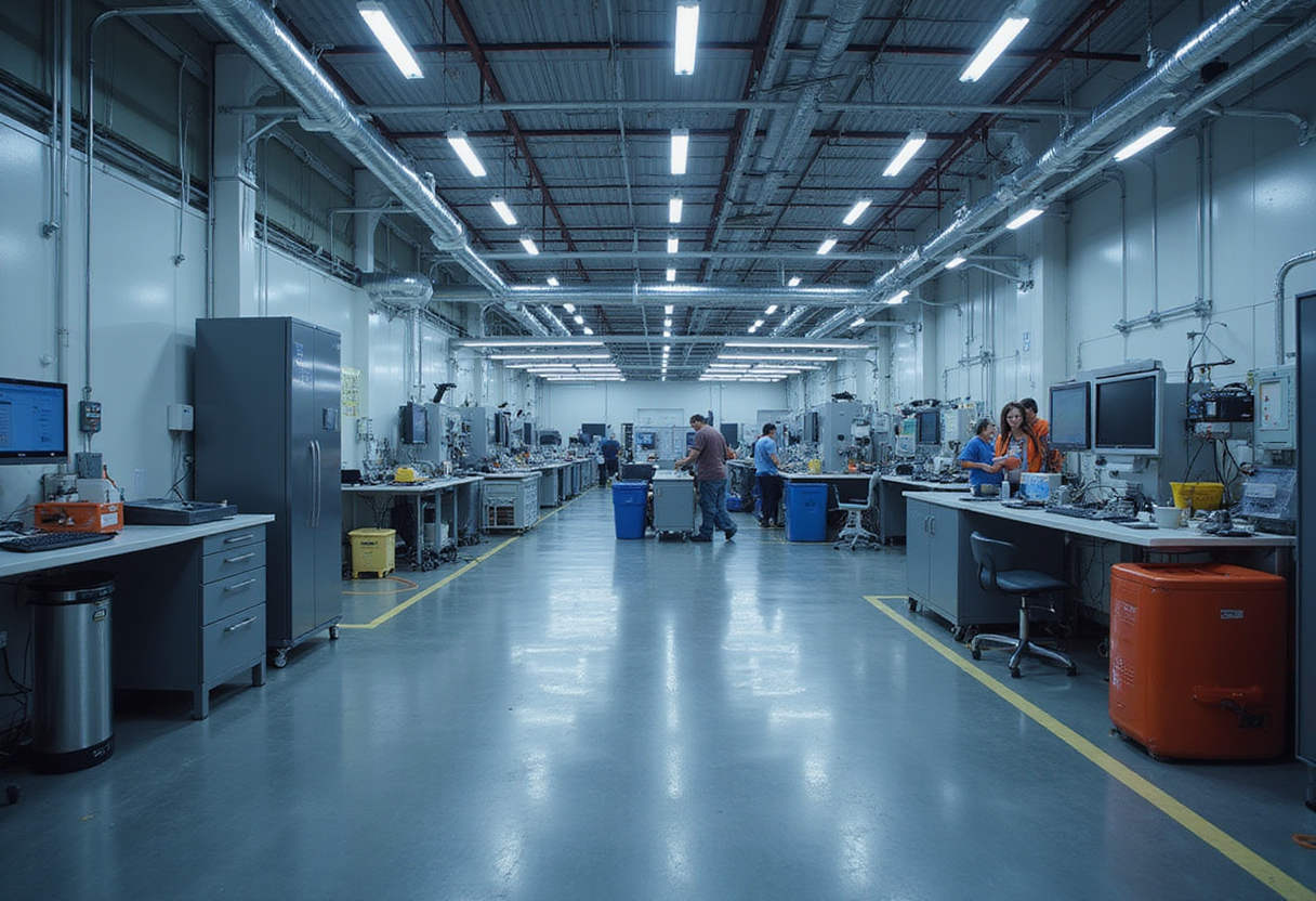
GlobalFoundries does not compete at the leading edge. Its business centers on differentiated nodes: RF silicon, embedded memory, power management and automotive-grade platforms on 200mm and 300mm wafers. Those segments supply automotive, IoT, aerospace and communications customers, sectors that drove the shortage-driven capacity commitments of recent years.
Why two fabs rather than one?
A two-fab structure suggests a staged or split build. Companies typically phase large projects to match demand signals and funding disbursements. It also gives the operator flexibility to separate process families or wafer sizes across sites.
The US-Japan framing adds a geopolitical dimension. Japan has been rebuilding its domestic chip base and coordinating with Washington on supply-chain resilience. A pact that routes new capacity through a US operator aligns both governments' stated goal of reducing concentration risk in advanced manufacturing.
What remains unspecified?
The announcement leaves key commercial parameters open:
- Fab locations and construction timelines
- Wafer sizes and target process platforms
- Investment value and funding split between governments and the company
- Committed capacity in wafers per month
Until those figures land, the deal stands as an operating agreement rather than a capacity commitment. Analysts will watch for the capital-expenditure number and any federal incentives attached, since those convert intent into schedulable output.
Competitive read
For GlobalFoundries, the pact strengthens its position in specialty foundry against rivals pursuing similar automotive and industrial sockets. Government backing lowers the financing risk that has historically constrained Western mature-node expansion. Rivals in Asia continue to add mature-node capacity aggressively, so timing will decide whether the new fabs arrive into a tight market or a glut.
The next milestones are site selection and a disclosed investment figure, which will set the pace for when the first wafers run.
Source: Google News: semiconductors
More from Grace Kim
Show full bio
Market editor covering people, launches and day-to-day practice in Semiconductors, chip manufacturing, hardware, AI compute at Chip Dispatch.
507 articles
Related articles
globalfoundries-to-run-new-york-fabs-under-us-japan-chip-initiative-cc789f25
GlobalFoundries to Run New York Fabs Under US-Japan Chip Initiative
japan-commits-up-to-21-billion-to-two-us-fabs-under-globalfoundries-c2e03fb4
Japan Commits Up to $21 Billion to Two US fabs Under GlobalFoundries
globalfoundries-to-run-two-new-york-fabs-under-u-s-japan-program-b943cf2d
GlobalFoundries to Run Two New York Fabs Under U.S.-Japan Program
globalfoundries-to-run-two-new-york-fabs-under-21-billion-plan-26687bae
GlobalFoundries to Run Two New York Fabs Under $21 Billion Plan