Infineon Processes First 300 mm Silicon Carbide Power Chips
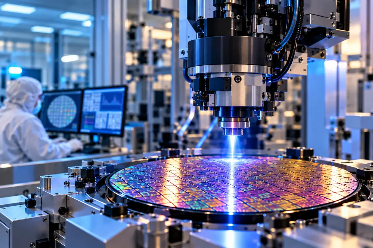
Infineon processed 300 mm SiC wafers into working power devices in Villach on existing silicon tools, claiming a first, but set no production date and gave no yield figures.
- By
- Nathan Brooks
- Filed
- Channel
- Chip Manufacturing
- Read
- 3 min read
Infineon has turned 300-millimeter silicon carbide wafers into functional power devices at its Villach fab in Austria, and claims to be the first company to do so in a full-scale semiconductor fab. The German chipmaker ran the wafers on existing silicon manufacturing equipment and is displaying the first processed wafer at the Electronica trade fair in Munich, which opened Tuesday.
The economics are arithmetic, not alchemy. A 300 mm wafer carries 2.3 times as many chips as a 200 mm wafer, Infineon said. The company offered no figures on yields or cost per chip, and set no production date. That is worth underlining: this is a demonstration, not a ramp.
What did Infineon actually prove?
Three things, each at a different site. First, the Villach result: 300 mm SiC processed into working power devices on tools already installed for silicon. That detail matters, because reusing depreciated equipment is the difference between a science project and a business case.
Second, Infineon said it has proved its Cold Split process on 300 mm SiC at its Dresden site. Cold Split separates wafers from a SiC crystal boule with less material loss and much shorter processing time than conventional wire sawing, so more wafers come from the same crystal. Silicon carbide is notoriously expensive to slice; any method that wastes less of the boule attacks the cost problem at its root.
Third, the company now holds 300 mm processes for all three power semiconductor materials: silicon, gallium nitride and silicon carbide. CEO Jochen Hanebeck put it plainly: "With silicon, gallium nitride and now silicon carbide 300-millimeter wafers, we are in a leading position to scale semiconductor manufacturing and drive profitable growth."
When will production start?
Infineon gave no date. The company will plan the 300 mm SiC technology and its ramp timing "in close collaboration with its customers and partners" while continuing its 200 mm SiC manufacturing roadmap. In practice, that means the incumbent 200 mm lines carry the revenue burden for now, and the larger wafer remains a roadmap item until customers commit.
The parallel with gallium nitride is instructive. On October 27, Infineon announced an investment of about €1.1 billion in high-volume manufacturing of GaN power chips on 300 mm wafers at Dresden. SiC has received no matching figure yet. The cheque, when it arrives, will be the real announcement.
Why does wafer size matter for SiC?
SiC switches power with lower losses than silicon at high voltages and temperatures. That property puts it in EV traction inverters, on-board chargers, EV chargers, grid-scale storage and industrial drives. Larger wafers cut the cost per die, which is the gate SiC must pass to move beyond premium applications.
The demand picture is shifting. Infineon names AI data centers alongside electric vehicles as a growth market, with SiC finding new roles in solid-state transformers, circuit breakers and power supply units. Data-center power is Infineon's fastest-growing business: on Tuesday the company forecast fiscal 2027 revenue of about €20 billion, with data-center power supply revenue approaching €4 billion.
What happens next?
Infineon must convert a working wafer into a qualified process, with yields and cost per chip it has so far declined to discuss. The 2.3x area advantage is real; whether it survives contact with SiC's difficult crystal economics is the question the Villach pilot line will now have to answer.
Source: mlq.ai
More from Nathan Brooks
Show full bio
Senior reporter covering people, launches and day-to-day practice in Semiconductors, chip manufacturing, hardware, AI compute at Chip Dispatch.
821 articles
Related articles
infineon-demonstrates-functional-sic-devices-on-300-mm-wafers
Infineon demonstrates functional SiC devices on 300-mm wafers
infineon-signs-200mm-sic-wafer-supply-deal-with-wolfspeed-7f8c8c3a
Infineon signs 200mm SiC wafer supply deal with Wolfspeed
infineon-puts-1-1-billion-into-world-s-first-300mm-gan-fab
Infineon Puts €1.1 Billion Into World's First 300mm GaN Fab
infineon-bets-1-1-billion-on-world-s-first-300mm-gan-fab-in-austria
Infineon Bets €1.1 Billion on World's First 300mm GaN Fab in Austria