NTT Docomo Business, Mitsubishi Estate Bet 13 Hectares on Chitose Chip Hub
NTT Docomo Business, Mitsubishi Estate and Chitose City will build a 13-hectare semiconductor R&D hub adjacent to Rapidus's plant, targeting partial opening in fiscal 2029. Costs are undecided.
- By
- Sophie Lindqvist
- Filed
- Channel
- Semiconductors
- Read
- 3 min read
Three partners will develop roughly 13 hectares of the Chitose Bibi World industrial park near New Chitose Airport into a next-generation semiconductor research hub, with a partial opening targeted for fiscal 2029. NTT Docomo Business, Mitsubishi Estate and Chitose City in Hokkaido signed the partnership agreement on the 23rd. Total project costs remain undecided.
The site sits directly adjacent to the Rapidus plant in Chitose, where the Japanese state-backed venture targets mass production of advanced semiconductors. The partners intend the new hub, named Chitose Technology Frontier (CTF), to anchor an industry-academia-government cluster around that plant.
What will the hub actually do?
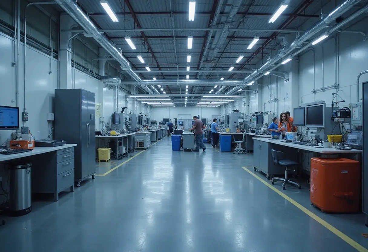
CTF will host integrated research and development across both halves of chipmaking. The front-end process etches fine circuitry onto substrates; the back-end process assembles chips into finished products. The site will provide an environment spanning the two, according to the agreement.
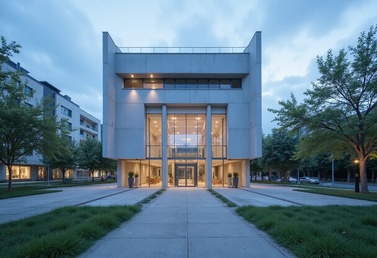
Plans call for multiple facilities: research buildings, offices and a museum, to be developed in phases. No budget figure, floor area or construction schedule beyond the fiscal 2029 partial opening has been published. That gap matters. Announcements of this kind routinely precede cost estimates by a year or more, and the partners have not said who pays for what.
Who brings what?
NTT Docomo Business will support semiconductor manufacturing centered on IOWN, the next-generation high-speed communications system promoted by its parent, NTT. The company claims IOWN will sharply reduce power consumed in production. It also expects that linking sites in Japan and overseas through high-speed communications will enable more efficient development.
Those claims come from the company itself. No power-reduction figure has been disclosed, and no independent estimate accompanies the announcement.
The telecom unit has moved quickly since Rapidus announced its Chitose expansion. It concluded a comprehensive partnership agreement with Chitose City in September on promoting the semiconductor industry and urban development. In June it signed an agreement with Kikuyo Town in Kumamoto Prefecture — home to a TSMC production site — aimed at deploying IOWN. The company now states it will support the revival of Japan's semiconductor industry from the communications-technology side at both locations.
Mitsubishi Estate's role is concrete infrastructure development. "We will actively take on cutting-edge technologies such as artificial intelligence (AI) and quantum computers," President Atsushi Nakajima said. Chitose Mayor Ryuichi Yokota said: "We will devote our efforts to realizing a world-class hub for advanced semiconductor research, development and innovation."
Why Chitose, and why now?
Development sites are already clustering around the Rapidus plant, including land tied to the National Institute of Advanced Industrial Science and Technology. Japan's government classifies semiconductors as a critical material for economic security and has strengthened the domestic production base with sustained subsidies.
The stated logic of concentration is layering. Grouping design, prototyping and workforce development functions around a mass-production site should, in the partners' view, compound capability rather than scatter it. The same clustering argument has driven TSMC's Kumamoto ecosystem, where NTT Docomo Business already holds its Kikuyo Town agreement.
What remains unresolved?
The framework prepares a host for advanced industry from two directions at once: communications infrastructure through NTT Docomo Business, and real estate development through Mitsubishi Estate. If semiconductor-related capital investment and corporate recruitment advance, Hokkaido could see expanded employment and demand across related industries, reshaping the regional industrial structure.
Two constraints sit alongside that promise. Securing power may emerge as a challenge, and so may securing workers — the source names both explicitly. Total project costs and facility details are still being finalized, and the specific division of roles among the parties will be a focus going forward.
For now, the fiscal 2029 date is a target, not a commitment. Whether CTF attracts semiconductor companies and universities from Japan and abroad, as intended, will depend on decisions the three partners have yet to publish.
Source: Google News: semiconductors
More from Sophie Lindqvist
Show full bio
News editor covering money, funding and market shifts around Semiconductors, chip manufacturing, hardware, AI compute at Chip Dispatch.
733 articles
Related articles
japan-us-weigh-chip-fab-buildout-inside-550b-investment-framework-10bde8b1
Japan, US weigh chip fab buildout inside $550B investment framework
chiayi-science-park-phase-3-breaks-ground-as-tsmc-eyes-five-more-packaging-plant-fa70f61e
Chiayi Science Park Phase 3 Breaks Ground as TSMC Eyes Five More Packaging Plants
globalfoundries-to-run-two-new-york-fabs-under-21-billion-plan-26687bae
GlobalFoundries to Run Two New York Fabs Under $21 Billion Plan
japan-and-us-weigh-19-billion-chip-plant-in-tariff-investment-pact-8dcdcf17
Japan and US Weigh $19 Billion Chip Plant in Tariff Investment Pact