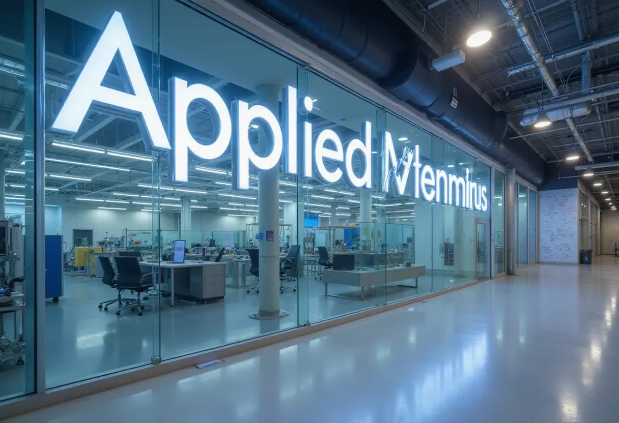
Applied Materials Opens $5 Billion Semiconductor Research Center in California
Applied Materials has opened a $5 billion semiconductor research center in California, a fab-scale bet on accelerating next-generation chipmaking equipment development in the US.
- By
- Grace Kim
- Filed
- Channel
- Chip Manufacturing
- Read
- 3 min read
Applied Materials has opened a $5 billion semiconductor research center in California, one of the largest dedicated research investments the chip equipment sector has seen on US soil.
The figure anchors a broader shift. Toolmakers, not just chipmakers, are now committing billions to domestic research infrastructure. Applied Materials supplies wafer fabrication equipment to leading logic and memory manufacturers worldwide. Its new center places process development work close to its Silicon Valley headquarters.
What does the facility do?
The center is a research hub. It brings together Applied Materials engineers, customers, and research partners under one roof. The company intends the site to accelerate development of next-generation process equipment and materials.
The investment covers the building and its research toolset. At $5 billion, the commitment ranks among the biggest single-site R&D outlays by any semiconductor equipment supplier. Few vendors in the sector operate research campuses at this scale.
Why California, and why now?
Applied Materials has deep roots in Silicon Valley. The company was founded there and built its core equipment business from the region. Locating the center in California keeps R&D adjacent to its existing engineering organization.
The timing matters. Demand for advanced chipmaking tools has surged as manufacturers expand capacity for leading-edge logic, memory, and packaging. Equipment research capacity has become a bottleneck in its own right. A dedicated facility shortens the loop between materials innovation and tool qualification.
The move also aligns with US policy pressure to strengthen domestic semiconductor infrastructure. Federal programs have pushed chipmakers and suppliers to expand American manufacturing and research. Equipment vendors benefit when their customers build fabs at home.
How large is the commitment?
The headline number is $5 billion. That places the project in the same weight class as major fab investments announced by chipmakers in recent years, though this sum funds research rather than volume production.
For comparison, that sum approaches the cost of a full production fab, which typically runs several billion dollars for mature nodes. Applied Materials is spending fab-scale money on development capacity alone. The bet signals confidence that process and materials research will drive the next decade of device scaling.
What it means for the supply chain
Chipmakers depend on Applied Materials for deposition, etch, and related process tools. Faster equipment development at the new center could compress timelines from laboratory concept to qualified production tool.
The facility also creates a US-based venue for collaborative research. Chip manufacturers, materials suppliers, and universities can work alongside Applied Materials teams. Such collaboration models have historically accelerated transitions between device generations.
For customers racing to advanced nodes, proximity to tool R&D reduces risk. Process changes at the leading edge increasingly depend on co-optimization of materials, equipment, and device design.
What comes next
Applied Materials has not detailed the center's full research agenda or staffing timeline in the announcement. The company will presumably publish milestones as programs at the site mature.
The opening strengthens Applied Materials' position as the sector's largest equipment vendor by revenue. Competitors will face pressure to match its research depth.
If the center delivers faster tool development cycles, the commercial effect will reach every major fab operator that runs Applied Materials equipment. The $5 billion wager now depends on whether materials and process breakthroughs at the site translate into qualified tools customers will buy.
Source: Google News: semiconductors
More from Grace Kim
Show full bio
Market editor covering people, launches and day-to-day practice in Semiconductors, chip manufacturing, hardware, AI compute at Chip Dispatch.
656 articles
Related articles
applied-materials-puts-5-billion-into-silicon-valley-r-d-center-16883488
Applied Materials Puts $5 Billion Into Silicon Valley R&D Center
applied-materials-commits-5-billion-to-silicon-valley-ai-chip-research-hub-0d3e3c8a
Applied Materials Commits $5 Billion to Silicon Valley AI Chip Research Hub
applied-materials-opens-5-billion-semiconductor-innovation-center-6136f976
Applied Materials Opens $5 Billion Semiconductor Innovation Center
applied-materials-puts-5-billion-into-silicon-valley-r-d-centre-aae52578
Applied Materials Puts $5 Billion Into Silicon Valley R&D Centre