Hanmi Semiconductor Opens US Hub for AI Packaging Customers
Hanmi Semiconductor has set up a US hub to support AI packaging customers, DigiTimes reports. No location, budget, or staffing figures were disclosed.
- By
- Sophie Lindqvist
- Filed
- Channel
- Chip Manufacturing
- Read
- 3 min read
Hanmi Semiconductor has established a United States hub to support its AI packaging customers, DigiTimes reported. The company, based in Seoul, supplies bonders used in advanced chip packaging. That equipment sits at the center of the current AI accelerator buildout. No dollar figure, headcount, or location for the hub appeared in the report.
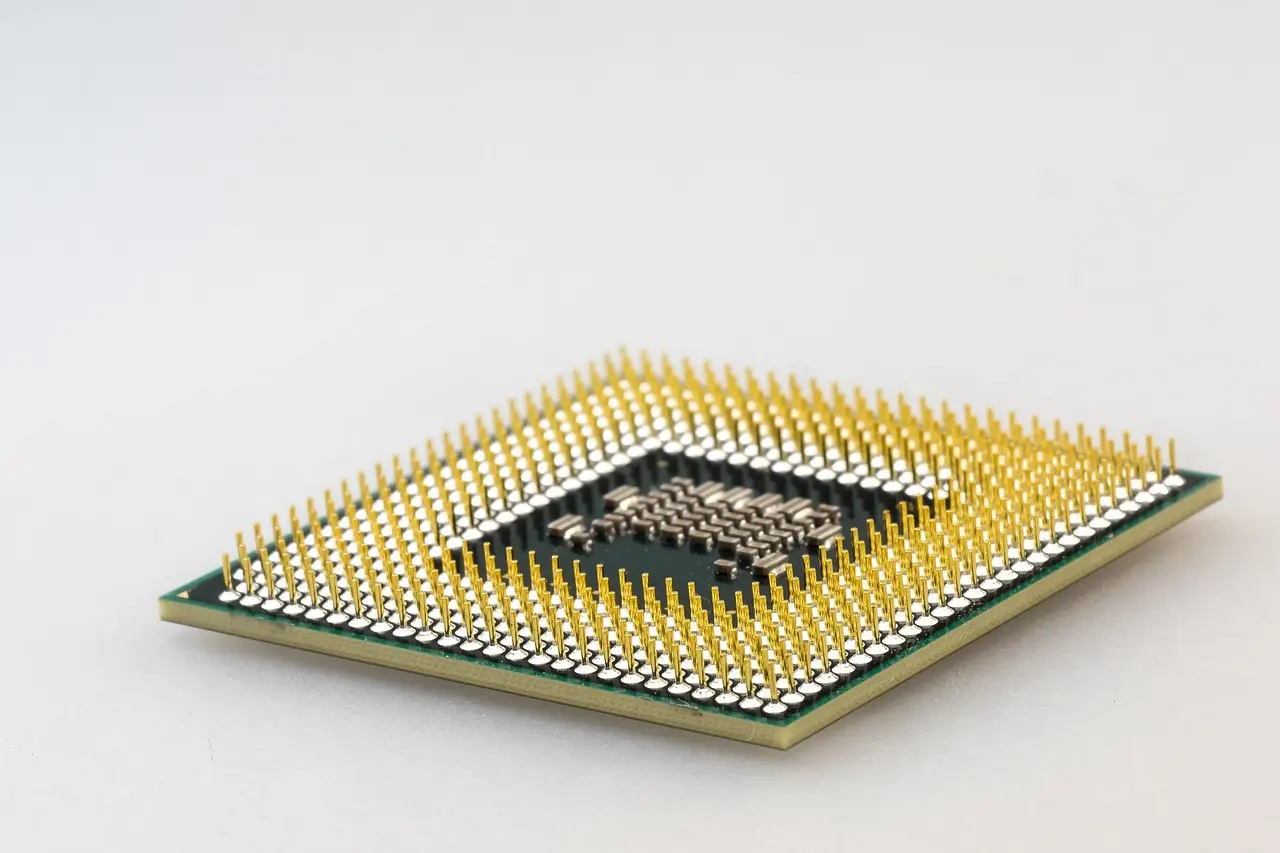
The move is small on paper. It is not small in signal. Advanced packaging, not lithography, has become the bottleneck for AI hardware. Hanmi's thermal compression bonders attach memory stacks and logic dies into the packages that Nvidia-class accelerators require. A service hub on US soil shortens repair and support cycles for customers racing to expand capacity.
Why does proximity matter now?
Packaging equipment fails on production clocks. When a bonder stops, an entire packaging line stops with it. Support from Korea means trans-Pacific shipping for parts and engineers. Support from a domestic hub means hours, not days. Hanmi has not stated which customers will use the hub. The company's known packaging customer base, however, overlaps heavily with the Korean and US memory and logic firms building high-bandwidth memory and advanced logic packages for AI systems.
The company has previously supplied bonders to SK hynix, a claim DigiTimes and Korean filings have repeated for years. SK hynix is the leading supplier of high-bandwidth memory, or HBM, the stacked DRAM used in nearly every current AI accelerator. If HBM output grows, bonder utilization grows with it. That arithmetic, not sentiment, explains the hub.
What is confirmed and what is not?
Confirmed: the hub exists, per DigiTimes. Confirmed: its stated purpose is support for AI packaging customers. Everything else remains unstated. The report offers no location, no staffing number, no investment amount, and no opening date. Readers should treat any larger strategic reading as inference until the company discloses more.
That restraint matters. Equipment makers often announce service outposts with modest budgets and frame them as expansion. Hanmi has not framed this one with numbers at all. The absence of a figure cuts two ways. Either the investment is genuinely small, or the company wants the announcement to travel further than the spend.
Where does this fit geopolitically?
Washington's chip subsidies have pulled packaging work toward the United States. The Commerce Department has pushed advanced packaging as a domestic priority, and customers increasingly ask suppliers for local support as fabs and packaging plants rise in Arizona, Texas, and New York. A Korean toolmaker placing staff in the US responds to that demand signal directly.
There is also a defensive angle. Korean equipment firms watched export controls redraw customer maps since 2022. A US service base keeps Hanmi close to the customers least exposed to those restrictions. The company has said none of this explicitly. The pattern is visible regardless.
What comes next?
The test of the hub will be response time, and customers will measure it quietly. If Hanmi later discloses an investment figure or names a site, that disclosure will show whether this is a service desk or a real footprint. For now, the announcement tells AI packaging buyers one concrete thing: their bonder vendor now stands on the same continent, and every future capacity claim from Hanmi deserves that same evidence-first scrutiny.
Source: Google News: semiconductors
More from Sophie Lindqvist
Show full bio
News editor covering money, funding and market shifts around Semiconductors, chip manufacturing, hardware, AI compute at Chip Dispatch.
652 articles
Related articles
hanmi-semiconductor-establishes-us-subsidiary-in-silicon-valley-4cc5f39d
Hanmi Semiconductor Establishes US Subsidiary in Silicon Valley
hanmi-semiconductor-opens-silicon-valley-subsidiary-to-chase-ai-packaging-b13c90bc
Hanmi Semiconductor Opens Silicon Valley Subsidiary to Chase AI Packaging
tsmc-plans-five-additional-advanced-packaging-plants-in-southern-taiwan-6c2b6e0c
TSMC Plans Five Additional Advanced Packaging Plants in Southern Taiwan
japanese-materials-giant-expands-china-chip-packaging-output-722d2b03
Japanese Materials Giant Expands China Chip Packaging Output