ASML and TSMC Push for Larger Photomasks to Pattern Smaller Chips
ASML and TSMC are pushing for larger photomasks to pattern smaller, denser chips, inverting scaling logic as reticle limits constrain large AI-class die designs.
- By
- Grace Kim
- Filed
- Channel
- Chip Manufacturing
- Read
- 3 min read
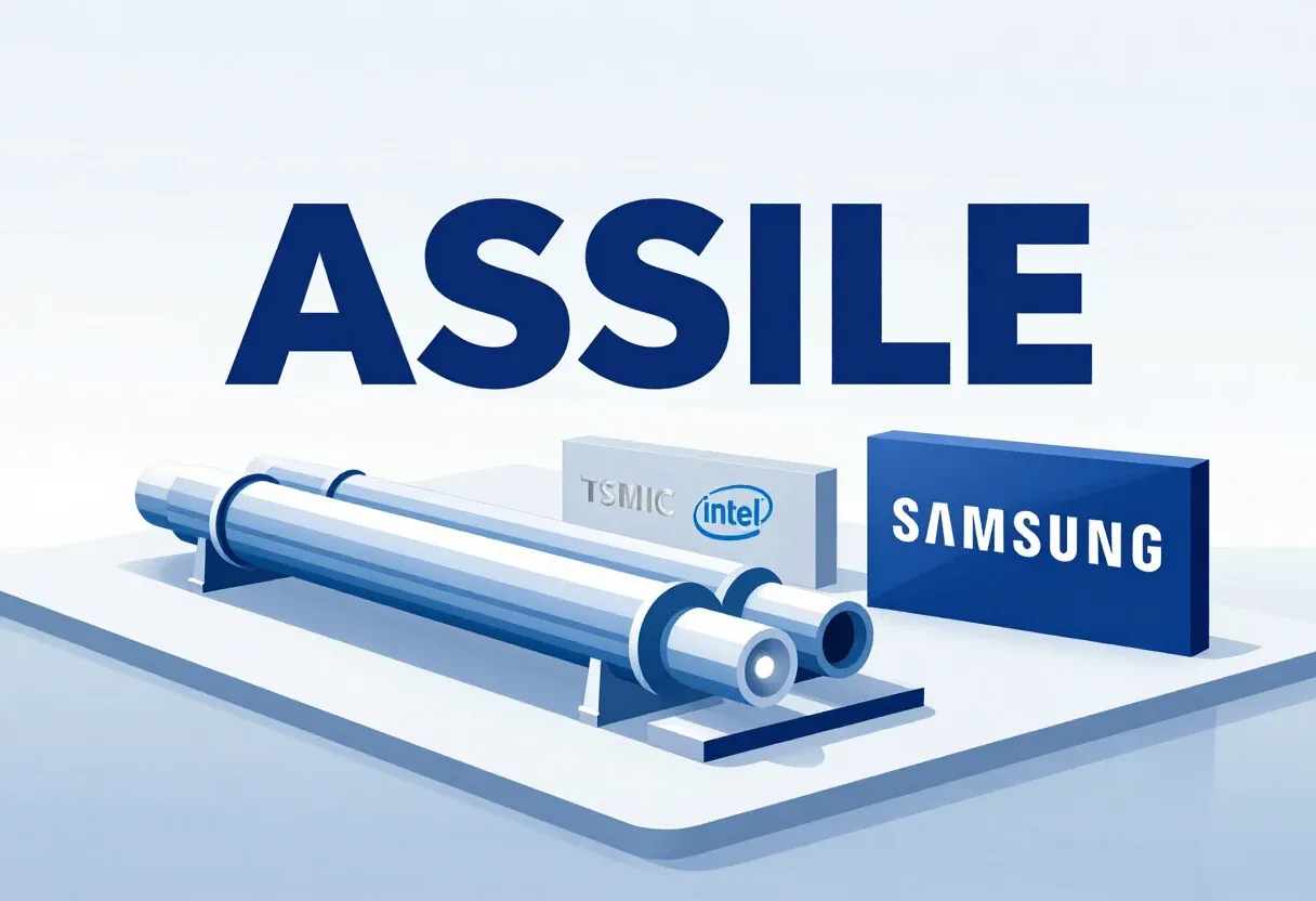
ASML and TSMC want bigger masks for smaller chips. That is the substance of a report by The Register, which says the lithography equipment maker and the world's largest foundry are seeking larger photomasks — the reticles that carry circuit patterns onto wafers — as a route to patterning ever-smaller features.
The proposal inverts the usual logic of semiconductor scaling. For decades the industry has shrunk features to pack more transistors onto each die. Now two of the industry's most powerful suppliers argue that enlarging the mask, not shrinking the tool, may be the more practical path to higher density.
Why would larger masks help make smaller chips?
A photomask sets an upper bound on the field size a lithography scanner can expose in a single shot. A larger mask permits a larger exposure field, and a larger field permits chip designers to place more circuitry in one exposure. That matters most for products whose dies approach the limits of today's reticle size, where designers must stitch multiple exposures together or split a design across several chips.
The push also reflects economics. Multi-patterning and stitching add process steps, add cost, and reduce yield. If a bigger mask lets a fab pattern a large die in fewer shots, the cost per wafer falls even before any change in transistor dimensions. The Register frames the ASML and TSMC effort as an engineering workaround aimed at this cost problem.
Who decides whether mask sizes change?
Mask and reticle dimensions are industry standards, not unilateral choices. Any move to a larger format would require coordination across toolmakers, mask blank suppliers, mask writers, inspection equipment vendors, and chip designers. ASML builds the scanners that project mask images onto wafers, so its scanners would need new optics and stages sized for a bigger reticle. TSMC, as the dominant advanced-node foundry, would be the most credible first customer for such a platform.
The report does not specify a target mask size, a timeline, or a process node where the change would first apply. It also does not quote executives from either company. The Register presents the effort as an ambition shared by the two companies rather than a confirmed roadmap item with committed dates.
What is at stake for the supply chain?
A larger mask format would ripple through the photomask supply chain. Mask blanks, e-beam mask writers, defect inspection tools, and pellicles are all built around the current reticle standard. Any enlargement would force capital investment at every layer of that chain, and suppliers would need confidence that volumes justify the outlay.
For TSMC, the commercial logic centers on leading-edge products. Large system-on-chip designs for artificial intelligence accelerators and high-performance processors already press against reticle limits, and CoWoS-class packaging multiplies the number of large dies a single product needs. A bigger exposure field would give designers more room per die.
For ASML, a new mask format could eventually drive a new class of scanner sales. The Dutch company holds a monopoly on extreme ultraviolet lithography tools, the machines that pattern the most advanced layers, and any change in exposure field size would flow through its product line first.
Is this a roadmap or an idea?
The Register's report establishes intent, not a schedule. There is no stated node, no announced tool, and no capacity figure tied to the proposal. Readers should treat the larger-mask concept as an industry direction under discussion between the two companies, distinct from confirmed investments such as fab construction or equipment orders.
The register of what is confirmed matters here. ASML and TSMC have not, in the material reported, committed engineering resources on a dated timeline. What exists is a shared argument that mask enlargement deserves a place in the scaling toolkit alongside transistor shrink and advanced packaging.
If the two companies convert the idea into a standards proposal with defined dimensions, the change would reshape reticle supply, scanner specifications, and design rules across the advanced-node ecosystem — and the pace of that decision will say much about how the industry plans to keep density gains coming.
Source: Google News: TSMC
More from Grace Kim
Show full bio
Market editor covering people, launches and day-to-day practice in Semiconductors, chip manufacturing, hardware, AI compute at Chip Dispatch.
673 articles
Related articles
asml-lines-up-intel-tsmc-and-samsung-behind-12-inch-masks-f70360a5
ASML Lines Up Intel, TSMC and Samsung Behind 12-Inch Masks
tsmc-claims-sole-5x-reticle-size-packaging-capability-says-it-can-absorb-rivals-5ab9d927
TSMC Claims Sole 5x Reticle-Size Packaging Capability, Says It Can Absorb Rivals' Shortfalls
engineering-the-world-s-largest-ai-chips-from-blueprint-to-build-fc0a88fe
Engineering the World's Largest AI Chips: From Blueprint to Build
digitimes-ai-scaling-shifts-from-die-shrinks-to-system-integration-2af5109e
DIGITIMES: AI Scaling Shifts From Die Shrinks to System Integration